Showing posts with label diagram. Show all posts
Showing posts with label diagram. Show all posts
Thursday, January 9, 2014
Simple Bilateral Current Source Circuit Diagram
Hi Friends ! I am sorry for dont update i post because i am busy few days. OK to day share with you Simple Bilateral Current Source Circuit Diagram This circuit uses a CA3193 precision op amp to deliver a current independent of variations in RL.
With RI set equal to R3, and R2 approximately equal to R4 + R5, the output current, h. is: VlN (R4)/(R3) (R5). 500-I`A load current is constant for load values from 0 to 3ohm.
Simple Bilateral Current Source Circuit Diagram


Saturday, December 21, 2013
5V Regulated Power Supply Circuit Diagram
This is a small +5V regulated power supply circuit. In that case here we used 7805 Voltage Regulator IC. 7805 is a +5 Volt regulator IC from 78xx chips family. The circuit has internal current limiting and thermal protection capacity. A 9V 2A steps down transformer is used to covert 230V to 9V from mains. Here used a bridge rectifier made by four 1N 4007 diode to convert AC-DC . 470uF 50v as C1 is used for filtering. This circuit is very easy to build. For good performance recommended input voltage 8V-18V. If over 400mA current is needed at output then use a heat sink with the 7805 IC.
Circuit diagram of 5V Regulated Power Supply
 |
| Fig-1: 5V regulated power supply schematic |
Pin Diagram of IC 7805
 |
| Fig2:Pin Diagram of IC 7805 |
Tuesday, December 17, 2013
Build a Power supply Protection Circuit Diagram
Why Build a Power supply Protection Circuit Diagram. When using a regulated supply to reduce a supply voltage there is always the danger of component failure in the supply and consequent damage to the equipment. A fuse will protect when excess current is drawn, but might be too slow to cope with over voltage conditions. The values shown are for a 12 V supply being dropped to 5 V.
Power supply Protection Circuit Diagram

The trip voltage is set to 5.7 V to protect the equipment in the event of a regulator fault. The 330 ohm resistor and the 500 ohm potentiometer form a potential divider which samples the output voltage as set by adjustment of the potentiometer. The SCR is selected to carry at least twice the fuse rating. The full supply voltage is connected to the input of the regulator.
The 2N2906 is held bias off by the 10 k resistor and the SCR so that the LED is held off. If the output voltage rises above a set trip value then the SCR will conduct, the fuse will blow, and the 2N3906 will be supplied with base current via the 10 k resistor, and the LED will light up.
Tuesday, October 8, 2013
AUDIO SCHEMATIC AND ROUTING ELECTRONIC DIAGRAM

AUDIO SCHEMATIC AND ROUTING ELECTRONIC DIAGRAM
It shows the connection and wiring between each parts and component of audio system of the vehicle such as the alternator, ignition switch, antenna meter, tail, audio, front speaker, rear speaker, tweeter speaker, and many more.
Sunday, October 6, 2013
METAL DETECTOR USING BEAT FREQUENCY OSCILLATOR ELECTRONIC DIAGRAM

METAL DETECTOR USING BEAT FREQUENCY OSCILLATOR ELECTRONIC DIAGRAM
The NAND gates use CMOS 4011 chip, a low power component that is suitable for this battery-operated circuit. You can see that this chip is supplied by a 5V voltage coming from an LM7805L regulator. You might wonder what the purpose of this regulation is, since the power supply come from a 9V battery and the CMOS gates can handle the voltage of 3-15 Volt. The main purpose of the regulator is to keep a constant voltage source for the reference oscillator frequency stability, since the frequency is affected by the power supply voltage variation as the battery voltage drops in the long time of usage.
This circuit uses parts as follows :
- U1: CD4011
- U2: LM389
- U3: 78L05
- R1: 2.2k 5%
- P2: 4.7k lin.
- R3: 330k 5%
- R4: 270k 5%
- R5: 1k 5%
- C1: 390pF (NPO)
- C2,C3,C4: 10nF
- C5: 10uF 16v electrolytic
- C6,C8: 220 uF 16v electrolytic
- C7: 100uf 16v electrolytic
- C9: 100nF ceramic
- P1: 4.7k log
- L1: 22cm in diameter with 14 turns AWG 26
- K1: SPDT toggle switch
- J1= Headphone jack 1/4 or 1/8 inch
- Other parts: 9v battery connector, speaker or headphones
Saturday, September 21, 2013
Fuse Box BMW 325i 1992 Convertible Power Distribution Diagram
Fuse Box BMW 325i 1992 Convertible Power Distribution Diagram - Here are new post for Fuse Box BMW 325i 1992 Convertible Power Distribution Diagram.

Fuse Panel Layout Diagram Parts: Service Interval Indicator, Tachometer/Fuel Economy Gauges, Gauges/Indicators;, Brake Warning System, Back Up Lights, On Board Computer, Start, Injection Electronics, Active Check Contro, Cruise Control, Injection Electronics, Radio/Antenna, Speedometer/Indicators, On Board Compute, Front Park/Tail, Horn, Rear Defogge, Injection Electronics, Ignition Key Warning/Seatbelt Warning, Auxiliary Fan, Auto Chraging Flashlight, Ignition Key Warning/Seatbelt WarninActive Check Control, Lights, Interior Lights , Central Locking, Radio/Antenna, On Board Computer, Cigar Lighter, Radio/Antenna, Heated/Air Conditioning, Active Check Control, Front Side Marker, Headlights, High Beam Indicator, Headlight, Auxiliary Fan, Lights, Turn/Hazard Warning, Wiper/Washer, Stop Lights, Active Check Control, Antilock Braking System;, Cruise Control, Map Reading Light, Headlights, Heated Seats, Power Windows, Auxiliary Fan, Auxiliary Fan, Interior Light, Power Mirrors, Injection Electronics, Interior Lights, Radio/Antenna, Trunk Light, Active Check Control, Service Interval Indicator, On Board Computer, Tachometer/Fuel Economy Gauge, Electro Mechanical Convertible Top.
Read the rest entry[...]
Fuse Box BMW 325i 1992 Convertible Power Distribution Diagram


Fuse Panel Layout Diagram Parts: Service Interval Indicator, Tachometer/Fuel Economy Gauges, Gauges/Indicators;, Brake Warning System, Back Up Lights, On Board Computer, Start, Injection Electronics, Active Check Contro, Cruise Control, Injection Electronics, Radio/Antenna, Speedometer/Indicators, On Board Compute, Front Park/Tail, Horn, Rear Defogge, Injection Electronics, Ignition Key Warning/Seatbelt Warning, Auxiliary Fan, Auto Chraging Flashlight, Ignition Key Warning/Seatbelt WarninActive Check Control, Lights, Interior Lights , Central Locking, Radio/Antenna, On Board Computer, Cigar Lighter, Radio/Antenna, Heated/Air Conditioning, Active Check Control, Front Side Marker, Headlights, High Beam Indicator, Headlight, Auxiliary Fan, Lights, Turn/Hazard Warning, Wiper/Washer, Stop Lights, Active Check Control, Antilock Braking System;, Cruise Control, Map Reading Light, Headlights, Heated Seats, Power Windows, Auxiliary Fan, Auxiliary Fan, Interior Light, Power Mirrors, Injection Electronics, Interior Lights, Radio/Antenna, Trunk Light, Active Check Control, Service Interval Indicator, On Board Computer, Tachometer/Fuel Economy Gauge, Electro Mechanical Convertible Top.
Friday, September 20, 2013
1995 Ford Ranger Wiring Diagram
 |
| 1995 Ford Ranger Wiring Diagram |
The Part of 1995 Ford Ranger Wiring Diagram: transmission range sensor, electronic engine control, clutch pedal position switch jumper, electronic engine control, speed control, automatic transmission, starter interupt relay, rela box, starter motor during engine starting, starter relay, manual transmission, electronic engine control, battery, starter motor solenoid, switch jumper, I/P fuse panel.
Tuesday, September 10, 2013
12V to 220V 100W Transistor Inverter Circuit Diagram
12V to 220V 100W Transistor Inverter Circuit Diagram

12V to 220V 100W transistor based power inverter.
Thursday, August 15, 2013
Simple Diodeless Rectifier Circuit Diagram
Simple Diodeless Rectifier Circuit Diagram. It`s common knowledge that when working with single-supply op amps, implementing simple functions in a bipolar signal environment can be difficult. Sometimes additional op amps and other electronic components are required. Taking that into consideration, can any advantage be attained from this mode The answer lies in this simple circuit (A). Requiring no diodes, the circuit is a high-precision full-wave rectifier with a liigli-frequency limitation equalling that of the op amps themselves.
Look at the circuit`s timing diagram (B) to see the principle of operation. The first amplifier rectifies negative input levels with an inverting gain of 2 and turns positive levels to zero.The second amp, a noninverting summing amplifier, adds the inverted negative signal from the first amplifier to the original input signal. The net result is the traditional waveform produced by full-wave rectification. In spite of the limitation on the input signal amplitude (it must be less than VCCJZ), this circuit can be useful in a variety of setups.
Diodeless Rectifier Circuit Diagram

Wednesday, August 14, 2013
Battery Charge Discharge Indicator Circuit Diagram
This Battery Charge-Discharge Indicator Circuit Diagram monitors car battery voltage. It provides an indication of nominal supply voltage as well as low or high voltage. RV1 and RV2 adjust the point at which the red/yellow and yellow/green LEDs are on or off. For example the red LED comes on at 11V, and the green LED at 12V. The yellow LED is on between these values.
Battery Charge-Discharge Indicator Circuit Diagram

Tuesday, August 13, 2013
Programmable Gain Amplifier Circuit Diagram
Programmable Gain Amplifier Circuit Diagram . The circuit uses the DG212 which controlling the gain using resistors. To calculate the different gains SW4 should be closed. Gain error is determined only by the resistor tolerance op amp offset and CMR will limit accuracy of circuit .
Programmable Gain Amplifier Circuit Diagram

Click here to download DG212.pdf datasheet.
Sunday, August 11, 2013
Wiring Diagram Electrical Components Symbols House Home

Electrical Wiring In The Home Wiring 2 Switches To 4 Lights.

Home Electrical Blueprint.

Electrical Floorplans With Power Low Voltage And Structured Wiring.

Home Electrical Wiring New Home Remodels Additions As You Wish.

Electrical Wiring In The Home Wires Are Not Hot In Electrical Outlet.

Home Electrical Wiring Trainers Kelvin Com.

Twelve Common Wiring Problems By Rex Cauldwell.

Electrical Wiring In The Home Wiring Nightmare Switch Phila.

All About Wiring Diagrams.

Wiring Diagram And Electrical Components Symbols For House Or Home.
Monday, August 5, 2013
USB Player Circuit Diagram
USB series player is an electronic device or electronic circuit that functions as an MP3 player that is stored on a storage device such as USB flash.
In this USB circuit using an IC as a modifier of digital voice data into analog so that it can be applied to a headphone, or again through the power amlplifier strengthened so that it can be heard through the speakers. IC used in this circuit using IC PCM2902 as a modifier of a digital data into analog data storage.
Below is a schematic diagram of a USB player

Thursday, August 1, 2013
Rj45 T568b Diagram Crosovercablea

Ethernet 100base T4 Crossover Cable Pinout And Wiring Pinouts Ru.

Terminating Wall Plates Structured Home Wiring.

Diagram 1 Residential Wiring.

There Are Two Acceptable Wiring Standards Tie Eia T568 A.

Rj45 T568b Diagram Crosovercablea Png.

Wiring Tutorial For 10baset Rj45 Unshielded Twisted Pair Utp.

Rj61 Wiring Color Code And Pinout Diagram Circuit Schematic.

Diagram Of Correct Color Alignment For Making Cat5e Network Cable.

Rj45 Jack 01 Jpg.

Clip Is Behind The Wiring Sequence Should Look Like This.
Wednesday, July 31, 2013
2005 3 5l Chevrolet Colorado Wiring Harness Diagram
The following schematic shows the 2005 3.5l Chevrolet Colorado Wiring Harness Diagram. This is a car powered by a straight, five cylinders engine or inline-five engine with 3.5L (3,460 cc/211 cu in) total displacement. The bore is 93 mm (3.7 in) and the stroke is 102 mm (4.0 in), this is a straight-five truck engine called the Vortec 350. It has long stroke (the stroke is longer than the bore) for better torque. (click image to enlarge)

LEGEND for the 2005 3.5l Chevrolet Colorado Wiring Harness Diagram:
(1) Accessory Switch C2
(2) Hazard Switch
(3) Accessory Switch C1
(4) Digital Radio Receiver (U2K)
(5) Inflatable Restraint I/P Module
(6) Ambient Light Sensor
(7) Vehicle Communication Interface Module (VCIM) (UE1)
(8) Courtesy Lamp – Footwell Right
(9) Body Control Module (BCM) C2
(10) C201 (I/P Harness to Body Harness)
(11) HVAC Control Module C1
(12) Auxiliary Power Outlet 2
(13) Auxiliary Power Outlet 1
(14) HVAC Control Module C2
(15) Courtesy Lamp – Footwell Left
(16) Data Link Connector (DLC)
(17) C204 (Steering Column Harness to I/P Harness)
(18) C208 (I/P Harness to Body Harness)
(19) C200 (I/P Harness to Body Harness)
(20) Headlamp and Panel Dimmer Switch
(21) Instrument Panel Cluster (IPC)
(22) Radio C1
(23) Radio C2
Friday, July 26, 2013
Build a Carrier Operated Relay Circuit Diagram
Carrier-Operated Relay Circuit Diagram shows a COR/CAS circuit for repeater use. CR1 is a silicon diode. 2 may be any relay with a 12-V coil (a long-life-reed relay is best). R2 sets the length of time that K2 remains closed after the input voltage disappears (hang time). shows a timer circuit. Values shown for Rl and CI should provide timing up to four minutes or so. CI should be a low-leakage capacitor; Ql is a silicon-controlled rectifier, ECG-5452 or equivalent.
Kl may be any miniature relay with a 12-volt coil. The timer is reset when the supply voltage is momentarily interrupted. The switch must be in the reset position for the remote reset to work. This circuit operates from the detector output of a receiver. A delay circuit is included so that the relay stays closed for a time period after the carrier output from the receiver disappears.
Carrier-Operated Relay Circuit Diagram

Saturday, July 13, 2013
LA4440 Bridge Amplifier Circuit Diagram
LA4440 is a dual channel audio amplifier IC. It can be used in two modes; one is Stereo amplifier and another Bridge amplifier mode. The LA4440 is a monolithic linear IC from Sanyo. Here I give the both circuit mode of amplifier using IC LA4440.
When the IC LA4440 is in Bridge mode in the circuit, its output power is 19w. In bridge mode use 4Ω-8Ω speaker. If you want stereo output(19w+19w) in bridge mode then use two copies of amplifier circuit of given below. Resistor R3&R4 is to adjust the voltage gain and for making input signal of inverting amplifier.

C10 is filter capacitor used to reduce the ripple of supply voltage. Don’t decrease the value of capacitor C6&C7 less than 100uF, 10v, it may causes of the output at low frequencies goes lower. The pin-6 of LA4440 amplifier circuit is audio input pin; it used in stereo amplifier mode but in bridge mode it is grounded. C8&C9 are polyester film capacitor used to preventing oscillation, and R1&R2 used for the same reason as filter resistor. Though the maximum supply voltage for both circuit of amplifier is 18V but we recommend to use a 12V,3A power supply. Use a good quality heat sink with LA4440.
I think here you see little comparison between stereo and bridge amplifier of LA4440. If you want to make this amplifier project, then I recommend you the bridge one. I think it is ideal for a beginner. And I love its wattage rather than Stereo mode. There is also a possibilities as I say, make two copies of circuit of bridge amplifier for stereo, it will give you 19w+19w of audio power output.
Tuesday, July 9, 2013
Simple Data accretion System Circuit Diagram
In this circuit, an HA-4900 series comparator is used in conjunction with a D/A converter to form a simple,

versatile, multichannel analog input for a data acquisition system. The processor first sends an address to the D/A, then the processor reads the digital word generated by the comparator outputs, lb perform a simple comparison, the processor sets the D/A to a given reference level, then examines one or more comparator outputs to determine if the inputs are above or below the reference. A window comparison consists of two such cycles with two reference levels set by the D/A. One way to digitize the inputs would be for the processor to increment the D/A in steps. The D/A address, as each comparator switches, is the digitized level of the input. While stairstepping, the D/A is slower than successive approximation; all channels are digitized during one staircase ramp.
Monday, July 8, 2013
230 Volt AC To Inverter Switching Circuit Diagram

Before three weeks i am introduced inverter circuit diagram but the circuit not included ac to inverter switching part so today i introducing a 230 Volt Ac to inverer switching circuit diagram .
Circuit showing a inverter switching . Here i have used bc 558 ,BC 548 and a relay for making this circuit . 230 volt connected to the base of the transistor Q1.When the power is ON positive volt coming to the base of the transistor so the relay circuit is open and load working in 230 V AC .When the power is OFF ground voltage coming to the base of the transistor so the Base of the Q2 is positive there for the relay circuit closed and load working in inverter input .Part list and applications are showing below.
Part List
| Component No: | Value | Usage |
| R1 | 100KΩ | Emitter Load |
| R2 | 10K Ω | Base Biasing |
| R3 | 180KΩ | Current Limiting |
| Q1 | BC558 | Switching |
| Q2 | BC548 | Switching |
| D1 | IN4007 | Relay Balancing |
| RL1 | 12 V | Inverter Switching |
Applications
* Inverter Switching
* AC Switching
Voltage to pulse Duration Converter Circuit Diagram
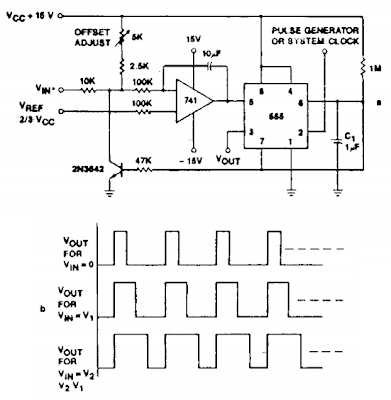
This is a circuit of Voltage-to-Pulse Duration Converter. This circuit is used to convert voltage into pulse duration by combining a timer IC and an OP Amp. Accuracies to better than 1% can be obtained with this circuit (a), and the output signals (b) still retain the original frequency, independent of the input voltage.
Voltage-to-pulse Duration Converter Circuit Diagram
Subscribe to:
Posts (Atom)