Showing posts with label converter. Show all posts

Tuesday, July 30, 2013

4 Bit Analogue to Digital Converter

The operation of the converter is based on the weighted adding and transferring of the analogue input levels and the digital output levels. It consists of comparators and resistors. In theory, the number of bits is unlimited, but each bit needs a comparator and several coupling resistors. The diagram shows a 4-bit version. The value of the resistors must meet the following criteria:
  • R1:R2 = 1:2;
  • R3:R4:R5 = 1:2:4;
  • R6:R7:R8:R9 = 1:2:4:8.
The linearity of the converter depends on the degree of precision of the value of the resistors with respect to the resolution of the converter, and on the accuracy of the threshold voltage of the comparators. This threshold level must be equal, or nearly so, to half the supply voltage. Moreover, the comparators must have as low an output resistance as possible and as high an input resistance with respect to the load resistors as feasible. Any deviation from these requirements affects the linearity of the converter adversely.
Circuit diagram:
4-bit_AnalogueTo_Digital_Converter-Circuit-Diagramw
4-Bit Analogue to Digital Converter Circuit Diagram
If the value of the resistors is not too low, the use of inverters with an FET (field-effect transistor) input leads to a near-ideal situation. In the present converter, complementary metal-oxide semiconductor (CMOS) inverters are used, which, in spite of their low gain, give a reasonably good performance. If standard comparators are used, take into account the output voltage range and make sure that the potential at their non-inverting inputs is set to half the supply voltage. If high accuracy is a must, comparators Type TLC3074 or similar should be used. This type has a totem-pole output. The non-inverting inputs should be interlinked and connected to the tap of a a divider consisting of two 10 kΩ resistors across the supply lines. It is essential that the converter is driven by a low-resistance source. If necessary, this can be arranged via a suitable op amp input buffer. The converter draws a current not exceeding 5 mA.
Source :www.extremecircuits.net
Read the rest entry[...]

Monday, July 8, 2013

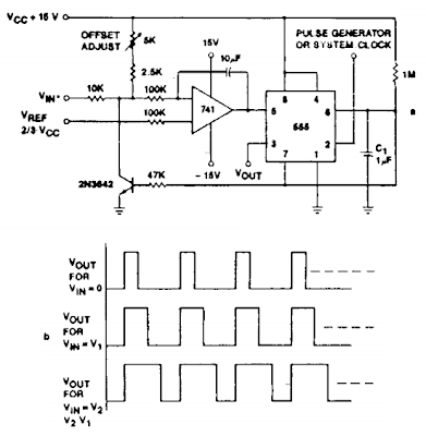
Voltage to pulse Duration Converter Circuit Diagram

This is a circuit of Voltage-to-Pulse Duration Converter. This circuit is used to convert voltage into pulse duration by combining a timer IC and an OP Amp. Accuracies to better than 1% can be obtained with this circuit (a), and the output signals (b) still retain the original frequency, independent of the input voltage. 

Voltage-to-pulse Duration Converter Circuit Diagram
 
Read the rest entry[...]

Saturday, April 13, 2013

Installtrailer Light Taillight Converter Towing

Trailer Wiring on Looking To The Rear For The Trailer Plug   The Pins Are Reversed   And
Looking To The Rear For The Trailer Plug The Pins Are Reversed And.


Trailer Wiring on Trailer Wiring Diagram Light Plug Brakes Hitch 4 Pin Way Wire Brake
Trailer Wiring Diagram Light Plug Brakes Hitch 4 Pin Way Wire Brake.


Trailer Wiring on Trailer Light Wiring   Typical Trailer Light Wiring Diagram
Trailer Light Wiring Typical Trailer Light Wiring Diagram.


Trailer Wiring on Trailer Parts Depot   Trailer Wiring Kits   Trailer Parts
Trailer Parts Depot Trailer Wiring Kits Trailer Parts.


Trailer Wiring on How To Install A Trailer Light Taillight Converter In Your Towing
How To Install A Trailer Light Taillight Converter In Your Towing.


Trailer Wiring on Wiring For 13 Pin Euro Plugs   Sockets For Trailers   Caravans   Uk
Wiring For 13 Pin Euro Plugs Sockets For Trailers Caravans Uk.


Trailer Wiring on Trailer Wiring Diagram
Trailer Wiring Diagram.


Trailer Wiring on Wiring Color For 7 Pin Trailer Plug Jpg
Wiring Color For 7 Pin Trailer Plug Jpg.


Trailer Wiring on Trailer Wiring Diagrams  Johnson Trailer Sales  Colfax Wisconsin
Trailer Wiring Diagrams Johnson Trailer Sales Colfax Wisconsin.


Trailer Wiring on 12s Wiring Diagram
12s Wiring Diagram.


Read the rest entry[...]

Wednesday, April 10, 2013

5V 2A Dc Converter Using LT3980

Using LT3980 manufactured by Linear Technology can be designed a very simple 5 volts dc converter circuit.

5V 2A Dc Converter Circuit Diagram


Converter Circuit Diagrams

The LT3980 has an adjustable frequency from 100kHz to 2.4MHz and accepts input voltages up to 58V . The transient voltage of the LT3980 is around 80 volts . The maximum output current which can be delivered by the LT3980 monolithic buck switching regulator is around 2 Amps .

Main features of the LT3980 monolithic buck switching regulator are : wide input range from 3.6V to 58V , overvoltage lockout protects circuits through 80V transients , 2A Maximum Output Current , low ripple (<15mVP-P) Burst Mode, aAdjustable switching frequency: 100kHz to 2.4MHz ,low shutdown current: IQ < 1μA, thermal protection, Soft-Start Capability . Link
Read the rest entry[...]

Monday, April 1, 2013

Serial To Parallel Converter

This converter may help if just the serial port on a personal computer is free, whereas the printer needs a parallel (Centronics) port. It converts a serial 2400 baud signal into a parallel signal. The TxD line, pin 3, CTS line, pin 8 and the DSR line, pin 6, of the serial port are used - see diagram. The CTS and DSR signals enable handshaking to be implemented. Since the computer needs real RS232 levels, an adaptation from TTL to RS232 is provided in the converter by a MAX232. This is an integrated level converter that transforms the single +5V supply into a symmetrical ±12V on.

Serial-to-Parallel Converter Circuit Diagramw

The serial-to-parallel conversion is effected by IC1. This is essentially a programmed PIC controller that produces a Centronics compatible signal from a 2400 baud serial signal (eight data bits, no parity, one stop bit). The IC also generates the requisite control signals. If there is a delay on the Centronics port, the RS232 bitstream from the computer may be stopped via the Flow signal (pin 17). This ensures that no data is lost. The controller needs a 4 MHz ceramic resonator, X1.

Source : www.extremecircuits.net

Read the rest entry[...]

Friday, March 29, 2013

Step Down Converter Controller

The TPS6420x controller is designed to operate from one to three series-connected cells or from a 3.3 V or 5 V supply obtained from a USB port. At its output it can produce 3.3 V at 2 A, suitable for powering a microcontroller-based system. With a suitable choice of external components (inductor, P-channel MOSFET and Schottky diode) the device can be operated over a wide range of possible output voltages and currents. A further advantage is its extremely low quiescent current consumption in power-down mode (100 nA typical) and in no-load operation (20 mA).

Also, if the input voltage is less than or equal to the desired output voltage, the device can connect the output directly to the input. Using just a few external components the TPS6420x can cover an output voltage range from 1.2 V up to the input voltage at up to 3 A, as long as a suitable P-channel MOSFET and Schottky diode are used. The device is an asynchronous step-down converter which, unlike the more widely-used PFM (pulse-frequency modulation) and PWM (pulse width modulation) types, involves a constant on-time and/or constant off-time.

Conventional controllers operate in PWM mode at medium to high loads, switching to PFM at lower loads in order to minimise switching losses. The controller described here also adjusts its switching frequency in accordance with the load to achieve a similar effect to the PFM/PWM controllers. The circuit diagram shows a classical step-down converter with an input voltage range from 3.3 V to 6 V and an output voltage of 3.3 V at a current of up to 2 A. The optional 33 m shunt resistor provides for current limiting.

Circuit diagram:
step-down converter controller circuit schematic

step-down converter controller circuit schematic

The TPS64202 offers a minimum on-time selectable between 1.6 ms, 0.8 ms, 0.4 ms and 0.2 ms and a fixed off-time of 300 ns. A MOSFET in the supply voltage path is switched on by the controller for as long as is necessary for the output voltage to reach its nominal value, or until the maximum permissible current, as determined by the shunt resistor, is reached. If the current does exceed this limit the MOSFET is switched off for 300 ns. If the nominal output voltage is reached, the MOSFET is switched off and remains in the off state until the output voltage once again falls below the nominal value.

At very low output currents the controller therefore operates in ‘discontinuous mode’ (DCM). Each switching cycle begins with the current at zero. It rises to the threshold or maximum value, and then falls again back to zero. At the moment of switch-off the Schottky diode causes the residual energy in the inductor to appear as a quickly-decaying oscillation at the resonant frequency of the output filter. This low-energy oscillation in discontinuous mode is normal and has no adverse effect on the efficiency of the converter.

It can be damped using the (optional) RC series network. At higher output currents the switch-down converter operates in continuous conduction mode (CCM). In this mode the inductor current never falls to zero. The output voltage is directly proportional to the switching mark-space ratio in this mode. If the Si2323 P-channel MOSFET from Vishay-Siliconix is not available, the IRLML6401 (12 V type) or IRLML6402 (20 V type) from IRF can be used instead.

Both these types have a higher on resistance, but do offer a lower gate capacitance. An alternative for the Schottky diode suggested is the MBRM140 (available from Digi-Key and Farnell), although this is in an SMB package rather than the Powermite package of the MBRM120. The voltage drop at 1 A is somewhat higher: 0.6 V instead of 0.45 V. The devices are manufactured by IRF and ON Semiconductor.

Literature at http://www.ti.com:
SOT23 Step-Down Controller, document reference number SLVS485
TPS6402 Evaluation Module (3.3 V, 2 A), document reference number SLVU093
Author: Dirk Gehrke
Read the rest entry[...]

Wednesday, March 27, 2013

6 to 15V DC to DC Converter

A very efficient 6V to 15V DC to DC converter using LM2585 is shown here. LM2585 is a monolithic integrated voltage converter IC that can be used in various applications like flyback converters, boost converters, forward converters, multiple output converters etc. The circuit requires minimum number of external components and the IC can source up to 3A output current.
Circuit diagram :
dc-to-dc-converter-Circuit Diagram
6 to 15V DC to DC Converter Circuit Diagram

Here the IC is wired as a boost converter where resistors R1 and R2 are used to set the output voltage .The junction of R1 and R2 is connected to the feedback pin of IC1. Capacitor C4 is the input filter while capacitor C1 the filter for output. Network comprising of resistor R1 and capacitor C2 is meant for frequency compensation. Inductor L1 stores the energy for acquiring boost conversion.
Notes:    
  • Assemble the circuit on a good quality PCB.
  • LM2585 requires a heatsink.
  • Output voltage is according to the equation Vout =( (R1/R2)+1) x 1.23.
  • Capacitors other than C4 and C1 are ceramic capacitors.
  • Maximum output current LM2585 can source is 3A. 

Source : Circuitstoday
Read the rest entry[...]