Showing posts with label circuit. Show all posts

Thursday, January 9, 2014

Simple Bilateral Current Source Circuit Diagram

Hi Friends ! I am sorry for dont update i post because i am busy few days. OK to day share with you Simple Bilateral Current Source Circuit Diagram This circuit uses a CA3193 precision op amp to deliver a current independent of variations in RL. 

With RI set equal to R3, and R2 approximately equal to R4 + R5, the output current, h. is: VlN (R4)/(R3) (R5). 500-I`A load current is constant for load values from 0 to 3ohm.

Simple Bilateral Current Source Circuit Diagram

Simple Bilateral Current Source Circuit Diagram

Read the rest entry[...]

Saturday, December 21, 2013

5V Regulated Power Supply Circuit Diagram

This is a small +5V regulated  power supply circuit. In that case here we used 7805 Voltage Regulator IC. 7805 is a +5 Volt regulator IC from 78xx chips family. The circuit has internal current limiting and thermal protection capacity. A 9V 2A steps down transformer is used to covert 230V to 9V from mains. Here used a bridge rectifier made by four  1N 4007 diode to convert AC-DC . 470uF 50v as C1 is used for filtering. This circuit is very easy to build. For good performance recommended input voltage 8V-18V. If  over 400mA current is needed at output then use a heat sink with the 7805 IC. 

Circuit diagram of 5V Regulated Power Supply

5V power voltage regulator
Fig-1: 5V regulated power supply schematic


 Pin Diagram of IC 7805


 7805 Pin Diagram
 Fig2:Pin Diagram
of  IC 7805

Read the rest entry[...]

Thursday, December 19, 2013

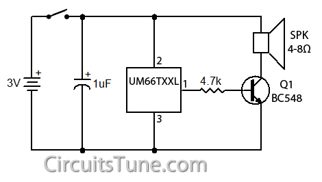
Song Music generator circuit using ic UM66

This is a simple (song) music generator circuit using ic UM66. To make a musical calling-bell, door-bell, kids toys etc. we can use this funny audio/sound/music/tone generator ic UM66. The UM66 series are CMOS IC’s, they has a built in ROM to store the music. The IC operates in DC +3V. We suggest to use two dry cell (1.5V X 2) for +3V Supply.  For Q1 use a TO-92 type NPN transistor like BC548, BC168, BC183, BC238, 2N2222. Speaker must be 4Ω or higher.

Circuit Diagram of Music generator using ic UM66: 

um66 music generator circuit
Fig: Circuit Diagram of Song-Music generator using IC-UM66


UM66TXX series IC generate different songs-music, the song-music depends on the model of UM66TXX series IC’s. The song-music are listed below with model number.

UM66TXX Songs List:
UM66T01 = Jingle Bells + Santa Claus is coming to town + Wish you a Merry Xmas
UM66T02 = Jingle Bells
UM66T04 = Jingle Bells + Rudolph, the red-nosed reindeer + Joy the world
UM66T05 = Home sweet home
UM66T06 = Let me call you sweetheart
UM66T08 = Happy birthday to you
UM66T09 = Wedding march
UM66T11 = Love me tender, Love me true
UM66T13 = Easter parade
UM66T19 = For Elise
UM66T32 = Waltz
UM66T33 = Mary had a little lamb
UM66T34 = The train is running fast
UM66T68 = Its small world
Read the rest entry[...]

Wednesday, December 18, 2013

Easy Loudspeaker Circuit For Telephone

This below circuit is a easy hands-free telephone receiver system. This doesn’t have dialing circuit so, it’s not a total phone replacement circuit, but it’s just only a loudspeaker system (i.e, phone receiver,not dialer). This is a easy circuit with all parts easily available, and without any complex I.C. It is made of just capacitors, diodes, resistors, and transistors.  This circuit can be made within 70 rupees and it compromises of the following sections,

Easy Loudspeaker Circuit For Telephone

  1. Power rectifier and filter section
    This section is made of a simple bridge rectifier and a indicating power LED.
  2. Voltage regulator section
    This section is made upon transistor Sl100, which is a general purpose NPN transistor in metal package. That is used to regulate voltage at a level of 9+0.6=9.6V by a 9V zener diode.
  3. Speaker output section
    This section contains a high impedance speaker and two BC548 NPN transistor to amplify the signal from line, the input of the 548 transistor pair is fed with a linear or pot control of 10K for volume adjust.
  4. Microphone input section
    This section contains a condenser microphone (tablet) and two BC548 NPN transistor to amplify the signal from mic, the output of the 548 transistor pair is fed with a linear or pot control of 10K for volume adjust to the line.
Read the rest entry[...]

Tuesday, December 17, 2013

Build a Power supply Protection Circuit Diagram

Why Build a Power supply Protection Circuit Diagram. When using a regulated supply to reduce a supply voltage there is always the danger of component failure in the supply and consequent damage to the equipment. A fuse will protect when excess current is drawn, but might be too slow to cope with over voltage conditions. The values shown are for a 12 V supply being dropped to 5 V.

Power supply Protection Circuit Diagram

Power supply Protection Circuit Diagram


The trip voltage is set to 5.7 V to protect the equipment in the event of a regulator fault. The 330 ohm resistor and the 500 ohm potentiometer form a potential divider which samples the output voltage as set by adjustment of the potentiometer. The SCR is selected to carry at least twice the fuse rating. The full supply voltage is connected to the input of the regulator.

The 2N2906 is held bias off by the 10 k resistor and the SCR so that the LED is held off. If the output voltage rises above a set trip value then the SCR will conduct, the fuse will blow, and the 2N3906 will be supplied with base current via the 10 k resistor, and the LED will light up.
Read the rest entry[...]

Tuesday, October 1, 2013

Egg Timer Circuit

This is a simple  egg timer circuit , which is both simple and functional, shows once again that it is not essential to use a microcontroller for everything these days. The circuit consists of only two ICs from the standard 4000 logic family, a multi-position rotary switch and a few individual components. The combination of a 4040 oscillator/counter and a 4017 decimal counter is certainly not new, but it is an ideal combination for timers that are required to generate long intervals that can be programmed in steps. The circuit can be directly powered from a 9-V battery, without using a voltage regulator. The signalling device is a 12-V buzzer, which generally works quite well even at a much lower voltage. We won’t explain the operation of the two ICs here; if you would like to know more about this, we recommend consulting the device data sheets.

The RC configuration has been selected for the oscillator circuit of the 4060, since the frequencies of standard crystals and resonators would be too high (even 32.768 Hz is much too high), making it impossible to achieve the desired times. With an RC oscillator, it’s also easier to modify the times to suit our purposes. For instance, if the oscillator frequency is reduced by a factor of two, we obtain a range of 1 to 16 minutes in steps of 1 minute. The range is split into two by taking advantage of the fact that the 4017 has an AND gate at its input (with an inverted input).The two ranges overlap by two steps. The oscillator has been dimensioned such that the 23 divider output (pin 14) has a period of 30 seconds, so IC2 receives a clock pulse every 30 seconds. This means that the oscillator frequency must be set to 8.5333 Hz.

Egg-Timer Circuit Diagram

The first output of IC2 is active after a reset, so it cannot be used. If S1 is in position I, pin 14 of IC2 is connected to the positive supply line. This input is used as an enable input. Directly after the first pulse from the 4060, the second output of IC2 goes high (which means after exactly half a minute). The sub-sequent outputs become active in turn at intervals of one clock pulse, and thus generate the states for 1 to 4.5 minutes. In the second range (II) of S1, the ‘enable’ pin of IC2 is connected to the 212 divider output of the 4060 (pin 1). This output goes high 4 minutes after the reset (which is why it is labelled ‘240 s’, instead of the period time of 480 s). Since the 4060 is an asynchronous counter, this output goes high a short time after the 23 output goes low. This delay provides the proper condition for an extra clock pulse for the 4017. The outputs of the 4017 will thus count upwards once. This means that the second output will become active after 4 minutes, with the rest of the outputs becoming active after 4.5 to 8 minutes. The desired timing interval is selected using switch S2.

graph-Egg_Timer

The output of S2 is connected directly to emitter follower T1, which energizes the buzzer when the level on the wiper of the switch is high. At the same time, the counter of IC1 is disabled via diode D1 by forcing the oscillator input high. The buzzer thus remains active until the circuit is switched off. The first counter output of the 4060 is connected to an LED (D2), which indicates that the circuit is active and the battery not yet exhausted. The blinking rate is approximately 0.5 Hz. The current through the LED is set to a modest 1mA, since this current represents the majority of the current drawn by the circuit.

This ranges from 0.5 to 1.5 mA, with the average current consumption being approximately 1mA while the timer is running. The buzzer used in our prototype increases the current to around 13 mA when it is energized, but this naturally depends on the actual type used. In principle, the circuit will work with any supply voltage between 3 and 16 V. However, the actual supply voltage should be taken into account in selecting the buzzer. The value of the supply voltage also has a small effect on the time interval, but in practice, the deviation proved to be less than 5 percent - which is not likely to matter too much to the eggs.

Read the rest entry[...]

Friday, September 27, 2013

Long Delay Timer Circuit

Suitable for battery-operated devices, Fixed 35 minutes delay

This timer was designed mainly to switch off a portable radio after some time: in this way, one can fall asleep on the sand or on a hammock, resting assured that the receiver will switch off automatically after some time, saving battery costs.

Circuit operation:

R1 and C1 provide a very long time constant. When P2 is momentarily closed, C1 discharges and the near zero voltage at its positive lead is applied to the high impedance inputs of the four gates of IC1 wired in parallel. The four paralleled gate outputs of the IC go therefore to the high state and the battery voltage is available at Q1 Emitter. When P2 is released, C1 starts charging slowly through R1 and when the voltage at its positive lead has reached about half the battery voltage, the IC gate outputs fall to zero, stopping Q1.

This transistor can directly drive a portable radio receiver or different devices drawing a current up to about 250mA. Connecting a Relay across the Emitter of Q1 and negative ground, devices requiring much higher voltage and current operation can be driven through its contacts. Pushing on P2 for 1 to 5 seconds, the circuit starts and then will switch off after about 35 minutes. This time delay can be varied by changing R1 and/or C1 values. P1 will stop the timer if required.
LED D1 is optional and can be useful to signal relay operation when the load is placed far from the timer.

Circuit diagram:

Long Delay Timer Circuit

Long Delay Timer Circuit Diagram

Parts:

R1_________10M 1/4W Resistor
R2_________4K7 1/4W Resistor
R3_________1K 1/4W Resistor (Optional, see Text)
C1_________220µF 25V Electrolytic capacitor
D1_________LED any type and color (Optional, see Text)
D2_________1N4148 75V 150mA Diode (Optional, see Text)
IC1_________4011 Quad 2 Input NAND Gate CMos IC (See Notes)
Q1_________BC337 45V 800mA NPN Transistor
P1,P2______SPST Pushbuttons
RL1________Relay with SPDT 2A @ 230V switch (Optional, see Text)
Coil Voltage 12V - Coil resistance 200-300 Ohm
Notes:

  • A 4011 Quad 2 Input NAND Gate was used for IC1, but many other CMos gates or inverter arrays can be used in its place, e.g. 4001, 4002, 4025, 4012, 4023, 4049, 4069. With these devices, all inputs must be tied together and also all outputs, as shown in the Circuit diagram.
  • The operating voltage of this circuit should lie in the 6 - 12V range.

Source: www.RedCircuits.com

Read the rest entry[...]

Wednesday, September 25, 2013

Battery powered Night Lamp Circuit

Ultra-low current drawing 1.5V battery supply

This circuit is usable as a Night Lamp when a wall mains socket is not available to plug-in an ever running small neon lamp device. In order to ensure minimum battery consumption, one 1.5V cell is used, and a simple voltage doubler drives a pulsating ultra-bright LED: current drawing is less than 500µA.
An optional Photo resistor will switch-off the circuit in daylight or when room lamps illuminate, allowing further current economy.
This device will run for about 3 months continuously on an ordinary AA sized cell or for around 6 months on an alkaline type cell but, adding the Photo resistor circuitry, running time will be doubled or, very likely, triplicated.

Circuit diagram :

Battery-powered Night Lamp Circuit diagram Battery-powered Night Lamp Circuit diagram

Parts:

R1,R2___________1M   1/4W Resistors
R3_____________47K 1/4W Resistor (optional: see Notes)
R4____________Photo resistor (any type, optional: see Notes)

C1____________100nF 63V Polyester Capacitor
C2____________220µF 25V Electrolytic Capacitor

D1______________LED Red 10mm. Ultra-bright (see Notes)
D2___________1N5819 40V 1A Schottky-barrier Diode (see Notes)

IC1____________7555 or TS555CN CMos Timer IC

B1_____________1.5V Battery (AA or AAA cell etc.)


Circuit operation:


IC1 generates a square wave at about 4Hz frequency. C2 & D2 form a voltage doubler, necessary to raise the battery voltage to a peak value able to drive the LED.


Notes:


  • IC1 must be a CMos type: only these devices can safely operate at 1.5V supply or less.

  • If you are not needing Photo resistor operation, omit R3 & R4 and connect pin 4 of IC1 to positive supply.

  • Ordinary LEDs can be used, but light intensity will be poor.

  • An ordinary 1N4148 type diode can be used instead of the 1N5819 Schottky-barrier type diode, but LED intensity will be reduced due to the higher voltage drop.

  • Any Schottky-barrier type diode can be used in place of the 1N5819, e.g. the BAT46, rated @ 100V 150mA.


Source : www.redcircuits.com

Read the rest entry[...]

Tuesday, September 24, 2013

Processor Fan Control Circuit

Fans in PCs can be objectionably loud. In many cases, the amount of noise produced by the fan can be considerably reduced by lowering its speed. Although this will decrease the amount of cooling, this need not be a problem as long as you don’t go overboard with slowing down the fan. Particularly with older-model processors, which consume quite a bit less power than the latest models, this trick can be used without any problems. This circuit is anyhow intended to be used with relatively old PCs, since more recent models generally have a fan control circuit already integrated into the motherboard. These controllers ensure that the amount of cooling is increased if the processor becomes too warm and decreased if the processor temperature is relatively low.

Circuit diagram:

Processor_Fan_Control_Circuit_Diagramw

Processor Fan Control Circuit Diagram:

The circuit described here consists of only a handful of components, which you will probably already have in a drawer some-where. Transistors T1 and T2 are driven into conduction by the base current flowing to the fan via P1 and D1. There will always be a current flowing through R1, and it will be approximately 120 times as large as the current through R2. R3 has been added to prevent the base current of T2 from becoming too large when P2 is set to its minimum resistance. D1 ensures that even at this extreme setting, the voltage on the base-emitter junction of T3 will still be large enough to allow it to conduct.

Read the rest entry[...]

Tuesday, September 10, 2013

12V to 220V 100W Transistor Inverter Circuit Diagram

 12V to 220V 100W Transistor Inverter Circuit Diagram

12V to 220V 100W Transistor Inverter

12V to 220V 100W transistor based power inverter.
Read the rest entry[...]

Thursday, August 15, 2013

Simple Diodeless Rectifier Circuit Diagram

Simple Diodeless Rectifier Circuit Diagram. It`s common knowledge that when working with single-supply op amps, implementing simple functions in a bipolar signal environment can be difficult. Sometimes additional op amps and other electronic components are required. Taking that into consideration, can any advantage be attained from this mode The answer lies in this simple circuit (A). Requiring no diodes, the circuit is a high-precision full-wave rectifier with a liigli-frequency limitation equalling that of the op amps themselves.

 Look at the circuit`s timing diagram (B) to see the principle of operation. The first amplifier rectifies negative input levels with an inverting gain of 2 and turns positive levels to zero.The second amp, a noninverting summing amplifier, adds the inverted negative signal from the first amplifier to the original input signal. The net result is the traditional waveform produced by full-wave rectification. In spite of the limitation on the input signal amplitude (it must be less than VCCJZ), this circuit can be useful in a variety of setups. 

 Diodeless Rectifier Circuit Diagram

Diodeless Rectifier Circuit Diagram
 
Read the rest entry[...]

Wednesday, August 14, 2013

Battery Charge Discharge Indicator Circuit Diagram

This Battery Charge-Discharge Indicator Circuit Diagram monitors car battery voltage. It provides an indication of nominal supply voltage as well as low or high voltage. RV1 and RV2 adjust the point at which the red/yellow and yellow/green LEDs are on or off. For example the red LED comes on at 11V, and the green LED at 12V. The yellow LED is on between these values.


Battery Charge-Discharge Indicator Circuit Diagram

Battery Charge-Discharge Indicator Circuit Diagram

Read the rest entry[...]

Tuesday, August 13, 2013

Programmable Gain Amplifier Circuit Diagram

Programmable Gain Amplifier Circuit Diagram . The circuit uses the DG212 which controlling the gain using resistors. To calculate the different gains SW4 should be closed. Gain error is determined only by the resistor tolerance op amp offset and CMR will limit accuracy of circuit . 

Programmable Gain Amplifier Circuit Diagram

Programmable Gain Amplifier Circuit Diagram


Click here to download DG212.pdf datasheet.

Read the rest entry[...]

Thursday, August 8, 2013

A Friendly Charger Circuit for Mobile Phones

Most mobile chargers do not have current/voltage regulation or short-circuit protection. These chargers provide raw 6-12V DC for charging the battery pack. Most of the mobile phone battery packs have a rating of 3.6V, 650mAh. For increasing the life of the battery, slow charging at low current is advisable. Six to ten hours of charging at 150-200mA current is a suitable option. This will prevent heating up of the battery and extend its life.

Circuit diagram:

A Friendly Charger Circuit  For Mobile Phones A Friendly Charger Circuit Diagram For Mobile Phones

Parts:

Resistors:
P1 = 10K LOG
R1 = 1K
R2 = 1K
R3 = 1K
R4 = 1K
R5 = 3.3K
R6 = 16R/2W
R7 = 220R
R8 = 3.3R
R9 = 1K

Capacitors:

C1 = 470uF/25V
C2 = 10uF/25V
C3 = 1KuF/25V

Semiconductors:

D1 = Red LED
D2 = Green LED
Q1 = BC547
Q2 = BD677
ZD1 = 12V/1W
ZD2 = 5.6V/1W
IC1 = CA3130

Description:

The circuit described here, provides around 180mA current at 5.6V and protects the mobile phone from unexpected voltage fluctuations that develop on the mains line. So the charger can be left ‘on’ over night to replenish the battery charge. The circuit protects the mobile phone as well as the charger by immediately disconnecting the output when it senses a voltage surge or a short circuit in the battery pack or connector. It can be called a ‘middle man’ between the existing charger and the mobile phone.

It has features like voltage and current regulation, over-current protection, and high- and low-voltage cut-off. An added specialty of the circuit is that it incorporates a short delay of ten seconds to switch on when mains resumes following a power failure. This protects the mobile phone from instant voltage spikes. When short-circuit occurs at the battery terminal, resistor R8 senses the over-current, allowing Q1 to conduct and light up D1. Glowing of D2 indicates the charging mode, while D1 indicates short-circuit or over-current status.

The value of resistor R8 is important to get the desired current level to operate the cut-off. With the given value of R8 (3.3 ohms), it is 350 mA. Charging current can also be changed by increasing or decreasing the value of R7 using the ‘I=V/R’ rule. Construct the circuit on a common PCB and house in a small plastic case. Connect the circuit between the output lines of the charger and the input pins of the mobile phone with correct polarity.

Author : D. Mohan Kumar Copyright : E F Y


Read the rest entry[...]

Monday, August 5, 2013

USB Player Circuit Diagram


USB series player is an electronic device or electronic circuit that functions as an MP3 player that is stored on a storage device such as USB flash.

In this USB circuit using an IC as a modifier of digital voice data into analog so that it can be applied to a headphone, or again through the power amlplifier strengthened so that it can be heard through the speakers. IC used in this circuit using IC PCM2902 as a modifier of a digital data into analog data storage.

Below is a schematic diagram of a USB player

Read the rest entry[...]

Friday, July 26, 2013

Build a Carrier Operated Relay Circuit Diagram

Carrier-Operated Relay Circuit Diagram shows a COR/CAS circuit for repeater use. CR1 is a silicon diode. 2 may be any relay with a 12-V coil (a long-life-reed relay is best). R2 sets the length of time that K2 remains closed after the input voltage disappears (hang time). shows a timer circuit. Values shown for Rl and CI should provide timing up to four minutes or so. CI should be a low-leakage capacitor; Ql is a silicon-controlled rectifier, ECG-5452 or equivalent. 

Kl may be any miniature relay with a 12-volt coil. The timer is reset when the supply voltage is momentarily interrupted. The switch must be in the reset position for the remote reset to work. This circuit operates from the detector output of a receiver. A delay circuit is included so that the relay stays closed for a time period after the carrier output from the receiver disappears. 

  Carrier-Operated Relay Circuit Diagram

 Carrier-Operated Relay Circuit Diagram
 
Read the rest entry[...]

Saturday, July 13, 2013

LA4440 Bridge Amplifier Circuit Diagram

LA4440 is a dual channel audio amplifier IC. It can be used in two modes; one is Stereo amplifier and another Bridge amplifier mode. The LA4440 is a monolithic linear IC from Sanyo. Here I give the both circuit mode of amplifier using IC LA4440.

When the IC LA4440 is in Bridge mode in the circuit, its output power is 19w. In bridge mode use 4Ω-8Ω speaker. If you want stereo output(19w+19w) in bridge mode then use two copies of amplifier circuit of given below. Resistor R3&R4 is to adjust the voltage gain and for making input signal of inverting amplifier.

LA4440 Bridge Amplifier Circuit Diagram

C10 is filter capacitor used to reduce the ripple of supply voltage. Don’t decrease the value of capacitor C6&C7 less than 100uF, 10v, it may causes of the output at low frequencies goes lower. The pin-6 of LA4440 amplifier circuit  is audio input pin; it used in stereo amplifier mode but in bridge mode it is grounded. C8&C9 are polyester film capacitor used to preventing oscillation, and R1&R2 used for the same reason as filter resistor. Though the maximum supply voltage for both circuit of amplifier is 18V but we recommend to use a 12V,3A power supply. Use a good quality heat sink with LA4440.

I think here you see little comparison between stereo and bridge amplifier of LA4440. If you want to make this amplifier project, then I recommend you the bridge one. I think it is ideal for a beginner. And I love its wattage rather than Stereo mode. There is also a possibilities as I say, make two copies of circuit of bridge amplifier for stereo, it will give you 19w+19w of audio power output.
Read the rest entry[...]

Friday, July 12, 2013

Simple 7805 Voltage Regulator Circuit

A voltage regulator is used to produce a constant linear output voltage. It’s generally used with AC to DC power supply. And also it can be used as well as a DC to DC voltage converter . To regulating low voltage, most used device is one single IC. 7805, 7812, 7905 etc. 78xx series are design for positive and 79xx series are for Negative voltage regulator.

7805 is a three terminal +5v voltage regulator IC from 78XX chips family. See 7805 pinout below. LM78XX series are from National Semiconductor. They are linear positive voltage regulator IC; used to produce a fixed linear stable output voltage.  National Semiconductor has also negative voltage regulator chips family, they indicate with LM 79XX. 78xx is used more than 79xx because negative voltage has a few usability purposes as we see.
I was previously posted a 5v regulated power supply circuit using 7805 IC, that circuit and this 7805 voltage regulator circuit is almost the same.
 
 
Its output voltage is +5V DC that we need. You can supply any voltage in input; the output voltage will be always regulated +5V. But my recommendation is, don’t supply more than 18V or less than 8V in input. There used two capacitors in this voltage regulator circuit, they aren’t mandatory to use. But it will be best if you use them. They helped to produce a smooth regulated voltage at output. Use electrolyte capacitor instead of ceramic capacitor.

One limitation of 7805 I have found that is its output current 1A maximum. Otherwise it is a good voltage regulator if you are happy with 1A. But if   you need over 400mA current in output then you should use a Heat Sink with IC LM7805. Otherwise it may fall damage for overheating.Link
 
Read the rest entry[...]

Wednesday, July 10, 2013

Linear RF Power Meter Circuit

The National Semiconductor LMV225 is a linear RF power meter IC in an SMD package. It can be used over the frequency range of 450 MHz to 2000 MHz and requires only four external components. The input coupling capacitor isolates the DC voltage of the IC from the input signal. The 10-k? resistor enables or disables the IC according to the DC voltage present at the input pin. If it is higher than 1.8 V, the detector is enabled and draws a current of around 5–8 mA. If the voltage on pin A1 is less than 0.8 V, the IC enters the shutdown mode and draws a current of only a few microampères. The LMV225 can be switched between the active and shutdown states using a logic-level signal if the signal is connected to the signal via the 10-kR resistor.
Circuit diagram:
linear-rf-power-meter-circuit-diagram1 Linear RF Power Meter Circuit Diagram
 
The supply voltage, which can lie between +2.7 V und +5.5 V, is filtered by a 100nF capacitor that diverts residual RF signals to ground. Finally, there is an output capacitor that forms a low-pass filter in combination with the internal circuitry of the LMV225. If this capacitor has a value of 1 nF, the corner frequency of this low-pass filter is approximately 8 kHz. The corner frequency can be calculated using the formula fc = 1 ÷ (2 p COUT Ro) where Ro is the internal output impedance (19.8 k?). The output low-pass filter determines which AM modulation components are passed by the detector.

rf-power-meter-circuit-diagram2 
The output, which has a relatively high impedance, provides an output voltage that is proportional to the signal power, with a slope of 40 mV/dB. The output is 2.0 V at 9 dBm and 0.4 V at –40 dBm. A level of 0 dBm corresponds to a power of 1 mW in 50 R. For a sinusoidal wave-form, this is equivalent to an effective voltage of 224 mV. For modulated signals, the relationship between power and voltage is generally different. The table shows several examples of power levels and voltages for sinusoidal signals. The input impedance of the LMV225 detector is around 50 R to provide a good match to the characteristic impedance commonly used in RF circuits.

The data sheet for the LMV225 shows how the 40-dB measurement range can be shifted to a higher power level using a series input resistor. The LMV225 was originally designed for use in mobile telephones, so it comes in a tiny SMD package with dimensions of only around 1 × 1 mm with four solder bumps (similar to a ball-grid array package). The connections are labelled A1, A2, B1 and B1, like the elements of a matrix. The corner next to A1 is bevelled.


http://streampowers.blogspot.com/2012/06/linear-rf-power-meter-circuit.html 
Read the rest entry[...]

Tuesday, July 9, 2013

Simple Mini Audio Amplifier circuit

Description

Here is a simple and humble 2 Watts mini audio amplifier circuit suitable for small pocket radios and other portable audio gadgets.The circuit is based on Phillips Semiconductors IC TDA 7052.The amplifier can be run even from a 3V Mercury button cell.This makes it ideal for battery operated gadgets.

The IC TDA7052 is a mono output amplifier coming in a 8-lead DI package (DIP). The device is mainly designed for battery-operated portable audio circuits. The features of TDA 7052 include ,no external components needed,  no switch-on or switch-off click sounds , great overall stability ,very low power consumption(quiescent current 4mA) , low THD, no  heat sinks required and short-circuit proof.

The gain of TDA 7052 is fixed internally at 40 dB. . To compensate the reduction of output power due to low voltage supply  the TDA7052 uses the Bridge-Tied-Load principle (BTL) which can provide  an output  of around 1 to 2 W  Rms(THD = 10%) into an 8 Ohm load with a power supply of 6 V.

In the circuit the potentiometer can be used to control the volume. Capacitor C1 and C2 are meant for  filtering the supply voltage if a battery eliminator is used as supply source. For operations using a battery C1 and C2 are not necessary.

Mini Audio Amplifier Circuit Diagram with Parts List:

mall Audio Amplifier Circuit

Notes.

  • Assemble the circuit on a good quality PCB or common board .
  • If you are a little expert, you can assemble the  circuit in a match box including the speaker.
Read the rest entry[...]