Showing posts with label amplifier. Show all posts

Wednesday, October 9, 2013

Hi Fi Headphone Amplifier

Contributed by Richard Crowley (Additional Notes by Rod Elliott

This design for a headphone amplifier arose after the purchase of commercial equipment with separate pre and power amplifiers without a headphone output.

It is based on designs for a headphone amplifier by John Linsley-Hood, and an active volume control, using a linear pot, by Doug Self (the "pot" circuit was originally designed by P.J. Baxandall), both published in Electronics and Wireless World in recent years.

Its advantages are ...

  • ow output impedance to drive several pairs of phones
  • the active gain stage is, almost, perfectly logarithmic and ...
    • is independent of the absolute value of the pot
    • has excellent channel tracking
    • the O/P noise reduces with gain reduction.
  • Description

    The intention is to permanently insert the headphone amp between pre and power amps, although it can be used as a stand-alone item. The input relay is operated by auxiliary contacts on the headphone sockets through a transistor driver (with a small delay) so as to mute the power amp input when listening on headphones.

    The relay contact arrangement enabling it (the headphone amp) to be left switched off when normally not in use. The relay is a high quality, sealed, gold plated contact, TQ signal switching type, reputedly with a very long life expectancy.

    The gain control being used to pre-set the gain so that the pre-amps gain control is normally used for setting the listening level.

    Hi-Fi Headphone Amplifier Figure 1 - The Headphone Amp Circuit

    One channel only is shown, so two units are required for stereo. The gain control pot must be a dual-gang linear type, as the circuit configuration provides the logarithmic law required. This is similar to the circuit shown in Project 01 (except that this version provides a useful reduction of noise). A value of 47k or 100k should be fine in this circuit. Diodes should be 1N4148.

    The first stage is a conventional series feedback circuit using the ubiquitous NE5534, the gain being set by the feedback AOT (adjust on test) resistor to suit individual needs, this stage provides the necessary low impedance output for the variable gain stage. The resistor/ capacitor networks around the input stage may seem a little extravagant, but are necessary to reduce any possible RF pickup especially the 470 pF between the two IC + and - inputs.

    The complete second stage consists of a zero gain follower, an inverting gain stage and the output emitter followers, volume control gain being set around these three stages. The x10 gain of the inverting stage gives the closest approach to a logarithmic law, stability being ensured by the 27pf capacitor in this stages feedback. The output complementary pair runs in Class-A at about 80 mA and should be mounted on a small heatsink.

    Dissipation is about 1.8 Watts for each device, and they must be isolated from the heatsink with mica washers and mounting bushes to prevent short-circuiting the power supply (the collectors are connected to the case). Make sure that heat-conducting paste is used, or use sil-pads for mounting - these require no thermal compound and are very convenient for low power operation.

    Figure 2 - Alternative Relay Driver, and Component Pinouts Figure 2 - Alternative Relay Driver, and Component Pinouts

    The OPA2604 was chosen because its high, FET based, input impedance provides better DC conditions for setting the O/P at 0V DC than the NE5532 alternative, its low output impedance has no problems in driving difficult loads, but it is still relatively cheap.

    The power supply is a fairly conventional split variety, the regulated O/Ps feeding the ICs - note the decoupling arrangements - and the 22V pre-regulated supply feeding the O/P transistors, the relay supply being rectified and regulated separately for the necessary isolation, separate signal and supply star earthing being essential

    Power  Supply Figure 3 - Power Supply

    The output jack sockets, with independent changeover contacts, are obtainable from Maplin Electronics and have proved extremely reliable over many years of regular use. If these are not obtainable a circuit is included for use with conventional break contact jack sockets.The LED series resistors will need to supply a current of about 7.5mA, so 2.2k should be used. Diodes for the supply should be 1N4004 or equivalent.

    If desired, the 12V regulator may be dispensed with, and suitable value resistors placed in series with each relay coil to retain the correct operating voltage. It is the constructors responsibility to determine the value of these, as the relay current cannot be predicted as there are so many different types available. Use of 15V relays is also possible, if available.

    If this arrangement is used, a slight amount of noise may be introduced as the relay operates, because of the sudden application (or removal) of the additional load. It is not expected that this would be a problem in use.

    My thanks to Richard for submitting this circuit - it is sure to provide a very high sound quality, and is not overly complex. The active gain control (originally designed by Peter Baxandall) is very effective.

    As always, resistors should be 1% metal film types for all signal paths. Their use in the power supply and relay circuits is not necessary, but will not do any harm, either.

    Source:www.sound.westhost.com

    Read the rest entry[...]

    Sunday, September 22, 2013

    Portable 9v Headphone Amplifier

    High Quality One-IC unit, Low current consumption
    After several requests by correspondents, the decision of designing a 9V powered Headphone Amplifier was finally taken. The main requirement was to power the circuit by means of a common, PP3 (transistor radio) alkaline battery. So, implementing a low current drawing circuit was absolutely necessary, though preserving a High Quality performance.

    Circuit Diagram:
    Portable 9v Headphone Amplifier Circuit Diagram
    Parts:
    P1 = 22K
    R1 = 18K
    R2 = 68K
    R3 = 68K
    R4 = 68K
    R5 = 18K
    R6 = 68K
    C1 = 4.7uF-25v
    C2 = 4.7uF-25v
    C3 = 22pF
    C4 = 220uF-25v
    C5 = 220uF-25v
    C6 = 4.7uF-25v
    C7 = 22pF
    C8 = 220uF-25v
    J1 = 3.5mm Stereo Jack
    B1 = 9V Alkaline Battery
    IC1 = NE5532-34
    SW1 = SPST Toggle Switch

    The appearance of the 5534 low-noise op-amp at a reasonable price was much appreciated by audio designers. It is now difficult or impossible to design a discrete stage that has the performance of the 5534 without quite unacceptable complexity. 5534 op-amps are now available from several sources, in a conventional 8-pin d.i.l. format. This version is internally compensated for gains of three or more, but requires a small external capacitor (5-15pF) for unity-gain stability. The 5532 is a very convenient package of two 5534s in one 8-pin device with internal unity-gain compensation, as there are no spare pins.

    The 5534/2 is a low-distortion, low-noise device, having also the ability to drive low-impedance loads to a full voltage swing while maintaining low distortion. Furthermore, it is fully output short-circuit proof. Therefore, this circuit was implemented with a single 5532 chip forming a pair of stereo, inverting amplifiers, having an ac gain of about 3.5 and capable of delivering up to 3.6V peak-to-peak into a 32 Ohm load (corresponding to 50mW RMS) at less than 0.025% total harmonic distortion (1kHz & 10kHz). If we consider that the mean current drawing at a power output of 15mW per channel is around 12-13mA (both channels driven), this Headphone Amplifier will become a must for many DIY enthusiasts needing a High Quality, High Performance portable device.

    Technical data
    Sensitivity:
        200mV RMS for 15.6mW RMS output
        350mV RMS for 50mW RMS output
    Maximum undistorted output: 3.6V Peak-to-peak
    Frequency response: flat from 40Hz to 20KHz; -2.3dB @ 20Hz
    Total harmonic distortion @ 1KHz: <0.025% at all power outputs up to 50mW RMS
    Total harmonic distortion @10KHz: <0.02% at all power outputs up to 50mW RMS
    Total current drawing @ 9V supply (both channels driven):
        Standing current: 8.5mA
        Mean current drawing @ 15mW RMS per channel: 12mA
        Mean current drawing @ 35mW RMS per channel: 17mA
     Source : www.redcircuits.com
    Read the rest entry[...]

    Friday, August 16, 2013

    18W Car Stereo Amplifier Rise

    This automobile stereo amplifier project is a class AB audio power amplifier using the Hitachi HA13118 module. It not only can be used in automobile application but also in any transportable or home amplifier process. It is simple to construct & has a maximum of outside parts. The module has a high power output from a low voltage supply using the bridge tied load system, & a high gain of 55dB.

    This project will be useful in applications where the input signal is a low level, without requiring the use of a separate pre-amplifier. This IC module has a built in surge protection circuit, thermal shutdown circuit, ground fault protection circuit & power supply fault protection circuit making it reliable.
    The Specifications of this project 
    D.C. Input : 8 – 18V at 1-2 A

    Power output : 18W maximum, 4 ohm load, 18V DC supply

    S/N ratio : > 70 dB

    THD : < 0.2% @ 1W

    Freq. Response : ~ 30 Hz to 30 kHz, –3 dB

    Input level : < 25 mV, for full output (G > 50dB)

    Input Impedance : ~ 30 k ohm

    The supply voltage necessary for this project is 8 -18V DC, at least one to two Amps. Maximum output power will only be obtained with a power supply of 18V at greater than two A, using a four ohm speaker. The power supply ought to be well filtered to reduce mains hum, a regulated supply will reduce noise even further. Additional filtering is unnecessary if operating from a battery supply.

    Circuit Diagram Description

    Most of the circuitry is contained within the amplifier module. C10 is the input coupling capacitor and blocks DC from the input. C11 bypasses any RF which may be present at the input. C1 & C2 provide an AC ground for the inverting inputs of the IC. R1/C7 and R2/C8 provide a high frequency load for stability with difficult speakers. C five & C six provide bootstrap feedback for the IC. C9 & C12 provide power supply filtering.


    An externally mounted logarithmic potentiometer of between 10k ohm and 50k ohm, is used depending on the desired input impedance. The impedance ought to be keep as high as feasible for a guitar amp, unless using a separate pre-amp. Make sure-that the heat sink is mounted to the module.


    Read the rest entry[...]

    Tuesday, August 13, 2013

    Programmable Gain Amplifier Circuit Diagram

    Programmable Gain Amplifier Circuit Diagram . The circuit uses the DG212 which controlling the gain using resistors. To calculate the different gains SW4 should be closed. Gain error is determined only by the resistor tolerance op amp offset and CMR will limit accuracy of circuit . 

    Programmable Gain Amplifier Circuit Diagram

    Programmable Gain Amplifier Circuit Diagram


    Click here to download DG212.pdf datasheet.

    Read the rest entry[...]

    Saturday, July 13, 2013

    LA4440 Bridge Amplifier Circuit Diagram

    LA4440 is a dual channel audio amplifier IC. It can be used in two modes; one is Stereo amplifier and another Bridge amplifier mode. The LA4440 is a monolithic linear IC from Sanyo. Here I give the both circuit mode of amplifier using IC LA4440.

    When the IC LA4440 is in Bridge mode in the circuit, its output power is 19w. In bridge mode use 4Ω-8Ω speaker. If you want stereo output(19w+19w) in bridge mode then use two copies of amplifier circuit of given below. Resistor R3&R4 is to adjust the voltage gain and for making input signal of inverting amplifier.

    LA4440 Bridge Amplifier Circuit Diagram

    C10 is filter capacitor used to reduce the ripple of supply voltage. Don’t decrease the value of capacitor C6&C7 less than 100uF, 10v, it may causes of the output at low frequencies goes lower. The pin-6 of LA4440 amplifier circuit  is audio input pin; it used in stereo amplifier mode but in bridge mode it is grounded. C8&C9 are polyester film capacitor used to preventing oscillation, and R1&R2 used for the same reason as filter resistor. Though the maximum supply voltage for both circuit of amplifier is 18V but we recommend to use a 12V,3A power supply. Use a good quality heat sink with LA4440.

    I think here you see little comparison between stereo and bridge amplifier of LA4440. If you want to make this amplifier project, then I recommend you the bridge one. I think it is ideal for a beginner. And I love its wattage rather than Stereo mode. There is also a possibilities as I say, make two copies of circuit of bridge amplifier for stereo, it will give you 19w+19w of audio power output.
    Read the rest entry[...]

    Friday, July 12, 2013

    100W Guitar Pre Amplifier Rise

    Introduction
    Guitar amplifiers are always an fascinating challenge. The tone controls, gain & overload characteristics are individual, & the ideal combination varies from guitarist to the next, & from guitar to the next. There is no amp that satisfies everyones requirements, & this offering is not expected to be an exception. The preamp is now at Revision-A, & although the whole schematic of the new version is not shown below, the essential characteristics are not changed - it still has the same tone control "stack" & other controls, but now has a second op amp to reduce output impedance & improve gain characteristics.

    One major difference from any "store bought" amplifier is that in case you build it yourself, you can alter things to fit your own needs. The ability to experiment is the key to this circuit, which is although introduced in complete form, there is every expectation that builders will make modifications to suit themselves.

    The amp is rated at 100W in to a four Ohms load, as this is typical of a "combo" type amp with 8 Ohm speakers in parallel. Alternatively, you can run the amp in to a "quad" box (four x 8 Ohm speakers in series parallel - see Figure five in Project 27b, the original editorial) and will get about 60 Watts. For the adventurous, two quad boxes and the amp head will provide 100W, but will be much louder than the twin. This is a common combination for guitarists, but it does make it hard for the sound man to bring everything else up to the same level.

    The Pre-Amplifier
    A picture of the Revision-A preamp is shown below. Youll see that theres dual op amps, but the schematic only shows. This is the main part of the Rev-A update - the output section now has gain (which is basically selected), and a better buffered low output impedance. The remainder of the circuit is unchanged.

    Guitar Pre-Amplifier Board

    The preamp circuit is shown in Figure one, and has a few fascinating characteristics that separate it from the "normal" - assuming that there is such a thing. This is simple but elegant design, that provides excellent tonal range. The gain structure is designed to provide a immense amount of gain, which is ideal for those guitarists who like to get that fully distorted "fat" sound.

    However, with a couple of simple changes, the preamp can be tamed to suit any style of playing. Likewise, the tone controls as shown have sufficient range to cover very anything from an electrified violin to a bass guitar - The response can be limited in the event you wish (by experimenting with the tone control capacitor values), but I recommend that you try it "as is" before making any changes.

    Figure 1 - Guitar Pre-Amplifier

    From Figure one, you can see that the preamp makes use of a dual op amp as its only amplification. The lone transistor is an emitter follower, & maintains a low output impedance after the master volume control. As shown, with a typical guitar input, it is feasible to receive a fat overdrive sound by winding up the volume, & then setting the master for an appropriate level. The general frequency response is deliberately limited to prevent extreme low-end waffle, & to cut the extreme highs to help reduce noise & to limit the response to the normal requirements for guitar. In case you use the TL072 op amp as shown, you may find that noise is an issue - at high gain with lots of treble boost. I strongly recommend that you use an OPA2134 - a premium audio op amp from Los angels Instruments (Burr-Brown division), you will then find this possibly the quietest guitar amp you have ever heard (or not heard :-). At any gain setting, there is more pickup noise from my guitar than circuit noise - & for the prototype one used carbon resistors!

    Notes:
    one - IC pin outs are industry standard for dual op amps - pin four is -ve supply, and pin 8 is +ve supply.
    two - Op amp supply pins must be bypassed to earth with 100nF caps (preferably ceramic) as close as feasible to the op amp itself.
    three - Diodes are 1N4148, 1N914 or similar.
    four - Pots ought to be linear for tone controls, & log for volume and master.

    The power supply section (bottom left corner) connects directly to the main +/-35V power amp supply. Use one Watt zen-er diodes (D5 and D6), and make positive that the zen-er supply resistors (R18 and R19, 680 ohm one Watt) are kept away from other parts, as they will get warm in operation. Again, the preamp PCB accommodates the supply on the board.

    The pin connections shown (either huge dots or "port" symbols) are the pins from the PCB. Normally, all pots would be PCB types, and mounted directly to the board. For a do-it-yourself project, that would limit the layout to that imposed by the board, so all connections use wiring. It may look a bit hard, but is simple and looks fine when the unit is done. Cable ties keep the wiring tidy, and only a single connection to the GND point ought to be used(several are provided, so select that suits your layout. VCC is +35V from the main supply, and VEE is the -35V supply.

    In the event you dont require all the gain that is available, basically increase the worth of R6 (the first 4k7 resistor) - for even less noise and gain, increase R11 (the second 4k7) as well. For more gain, decrease R11 - I recommend a maximum of 2k2 here.


    If the bright switch is bright ( much treble), increase the 1k resistor (R5) to tame it down again. Reduce the worth to get more bite. The tone control arrangement shown will give zero output if all controls are set to maximum - this is unlikely to be a common requirement in use, but be aware of it when testing.

    The diode network at the output is designed to permit the preamp to generate a "soft" clipping characteristic when the volume is turned up. Because of the diode clipping, the power amp needs to have an input sensitivity of about 750mV for full output, otherwise it wont be feasible to get full power even with the Master gain control at the maximum setting.

    Make positive that the input connectors are isolated from the chassis. The earth isolation parts in the power supply help to prevent hum ( when the amp is connected to other mains powered equipment).
    If issues are encountered with this circuit, then you have made a wiring mistake .. period. A golden rule here is to check the wiring, then keep on checking it until you find the error, since I can assure you that if it does not work properly there is at least mistake, & probably more.


    The input, effects & output connections are shown in Figure 1B.

    Figure 1B - Internal Wiring

    The connections shown are similar (ok, virtually identical :-) to those used in my prototype. Noise is low, & probably might have been lower if I had made the amp a tiny bigger. All connectors must be fully insulated types, so there is no connection to chassis. This is important !

    You will notice from the above diagram that I didnt include the "loop breaker" circuit shown in the power supply diagram. For my needs, it is not necessary, for your needs, I shall let you pick. In case you select to make use of it, then the earth (chassis) connection marked * (next to the input connectors) must be left off.

    A few important points
    The main 0 volt point is the connection between the filter caps. This is the reference for all zero volt returns, including the 0.1 ohm speaker feedback resistor. Dont connect the feedback resistor directly to the amps GND point, or you will generate distortion & feasible instability.
     The supply for the amp & preamp must be taken directly from the filter caps - the diagram above is literal - that means that you follow the path of the wiring as shown.
     Although mentioned above, you might well ask why the pots dont mount directly to the PCB to save wiring. Simple . Had I done it that way, you would require to make use of the same type pots as I designed for, & the panel layout would must be the same , with the exact same spacings. I figured that this would be limiting, so wiring it is. The wiring actually doesnt take long & is simple to do, so is not an issue.
     I didnt include the "Bright" switch in Figure 1B for clarity. I expect that it will cause few issues.


    Read the rest entry[...]

    Tuesday, July 9, 2013

    Simple Mini Audio Amplifier circuit

    Description

    Here is a simple and humble 2 Watts mini audio amplifier circuit suitable for small pocket radios and other portable audio gadgets.The circuit is based on Phillips Semiconductors IC TDA 7052.The amplifier can be run even from a 3V Mercury button cell.This makes it ideal for battery operated gadgets.

    The IC TDA7052 is a mono output amplifier coming in a 8-lead DI package (DIP). The device is mainly designed for battery-operated portable audio circuits. The features of TDA 7052 include ,no external components needed,  no switch-on or switch-off click sounds , great overall stability ,very low power consumption(quiescent current 4mA) , low THD, no  heat sinks required and short-circuit proof.

    The gain of TDA 7052 is fixed internally at 40 dB. . To compensate the reduction of output power due to low voltage supply  the TDA7052 uses the Bridge-Tied-Load principle (BTL) which can provide  an output  of around 1 to 2 W  Rms(THD = 10%) into an 8 Ohm load with a power supply of 6 V.

    In the circuit the potentiometer can be used to control the volume. Capacitor C1 and C2 are meant for  filtering the supply voltage if a battery eliminator is used as supply source. For operations using a battery C1 and C2 are not necessary.

    Mini Audio Amplifier Circuit Diagram with Parts List:

    mall Audio Amplifier Circuit

    Notes.

    • Assemble the circuit on a good quality PCB or common board .
    • If you are a little expert, you can assemble the  circuit in a match box including the speaker.
    Read the rest entry[...]

    Saturday, July 6, 2013

    100 W Bipolar Power Amplifier

    This is a basic 100 watt power amplifier designed to be (relatively) easy to build at a reasonable price. It has a better performance (read: musical quality) than the standard STK module amps that are used in almost every mass market stereo receiver manufactured today.

    100 W Bipolar Power Amplifier Circuit Diagram


    When I originally built this thing, it was because I needed a 100 WPC amp and do not want any money. So I designed around parts I had in the store. The design is actually a standard format, and I’m sure there are commercial entities that are similar. To my knowlwdge, it is not an exact copy of a commercial entity, nor am I aware of any patents on topology.

    For experienced builders: I am aware that many improvements and adjustments can be made, but the idea was to keep it simple and must do-able by anyone who is a circuit, and has not the patience to do a sloppy job. If friend want Bipolar Transistor power amplifier circuit. , In model HIFI OCL 100W RMS. I think this track should be an interesting choice, this circuit is the use of the key transistor BD317 and BD318 unless transistor number BD139, BD140, BC556 too easy then try to buy when the 35V power source with only then build is not difficult for other details as the result of a few See Circuit.

    Input stage is a BC556 transistor, which most of the open loop gain, and on the serene DC voltage stabilizes. This feeds a level shift stage where the voltage swing to (-) track references. The Transconductance stage is a Darlington, improve frerqency high linearity. The BD317, 318 on a rather large collector-base capacity is dependent on voltage. The BD319 presents this low-z and has a C (ob) of only a few of PF, which is effectively swamped by the pole-splitting 220pF cap. The scene is supplied by BC546 active load (current), which is approximately 20 mA. The current, until the BC556 is limited to about 70 mA in the worst cases.
    Read the rest entry[...]

    Thursday, May 2, 2013

    22 Watt Stereo Amplifier

    This circuit is very basic to build and puts out great power for your car or home. Keep all leads as short as possible

    22 Watt Stereo Amplifier circuit diagram
    Read the rest entry[...]

    Monday, April 8, 2013

    Tips and Tricks on Audio Power Amplifier Circuit

    Amplilfier power series from the beginning until now did not experience any changes. Some say this series is good, but the series was good fitting assembly and tested the results are not as we expected.
    The problem is usually treble is less subtle, less sound, sound breaking, buzz, middle of the field tested the bass sound is lost. so you do not have to believe what people 100%. The quality amplifier built-up would differ greatly with the amplifier assembly, a series can be the same but the quality will depend on who manufacture it.

    Here are a few tricks to try

    How to cope with a buzzing sound
    Power amplifiers are often used in the field blazer. This circuit is said said person is a bell assembly. But you do not immediately interested in this power, the circuit rather complicated and difficult to understand reflect the intelligence of people who first mendisainnya. In my opinion a great power is the power of simple, inexpensive, easily assembled and rational. You do not need to use expensive components such as the price of tantalum capacitors, power mosfet and the other expensive. This does not determine the quality of the power amp so that we raft. Power of sometimes causing buzzing, to overcome that is by holding the line input jack ground to the ground with 10-22 ohm resistors. So do not just take the ground input from the ground but held first with the R 10 ohms.


    How to setting bias trimpot
    Rotate the trimpot bias (if any) until the drain current of 50-100mA on each power transistor, in order to avoid defects treble in volume in the top position at 10. The risks are so panassss heatsink! (This setting marks on plate A-AB)

    Offset trimpot setting
    At the time of input without a signal, turn the trimpot so that the voltage on the speaker offsets actually read 0 volts. If you do not want to bother, use and entrust it with ic type series from Hitachi HA17741 IC brand quality or other! This is the heart of the series, 90-95% of quality is determined from the IC circuit this!

    Overcoming the voice
    Use pre-amp circuit to increase the signal of at least 2 times. normally and should pre-amp circuit uses IC op-amps with +12 V minimum supply-12V. Raise his mid tone!
    If hard you do not want to just use the tone control circuit IC is his mid!
    The secret is not in his mid tone alone, but the signal output from the IC op-amps are usually large.

    Treble rupture
    Excessive treble will damage the power amp, power rather than out even ngedrop. Handle, attach the filter capacitor on the input 1NF power amp to ground to ensure the signal is not disabled. Always use a quality active components such as ICs and transistors, 500 price difference will also be different results.
    Use a large cable and short as possible, especially for leg power transistor, and this transistor should be directly soldered to the pcb.

    Missing bass in field
    Usually power for field use supplay CT 50V 50V transformer, or at least 42V 42V ct. The greater the greater the supply voltage watt channeled though the series is written only 300-400 Watts only. This course uses Elko capacitors with voltage 80-100V. 10.000uF/100V capacitor will be equal to 4X10.000uF/50V and of course voltage capacitor is filled with full / almost full.
    Try to use a strong Elko at temperatures of 105 C. Capacitors are strong in supply of more than nominal voltage is written on his body. For example 4700uF/50V 85C capacitor will quickly explode in voltage 51V 85C. And Elko will be strong 105C 4700uF/50V voltage supplied more than 50V at a temperature of 85C. Elco so that it does not quickly explode if given the full voltage, keep its temperature as cold as possible, fan with the cool air.

    For speaker
    Try using a driver speakers that have a large spool diameter fitted with a suitable size bok. Usually included examples of the parameters / dimensions bok. Size bok bok2 usually larger than that sold in the market. if you force using bok that from this market, use driver type G12-80 (sorry no fear brand called promotion) speakers with bass tones to wall size small. Bok wall should be thick, strong and do not forget glued! Bok who will not be glued with a different sound, especially bass tones, prove it!

    Heat Sensor
    The form of transistor, the transistor is usually type BD139 MJE340 or it could be located in the center, flanked by a pair of transistors having a certain equal. These transistors must be mounted on the main heatsink to detect the heat generated by power transistors. It acts to lower bias currents at the hot heatsink. So what heatsink and power transistors must be set diposisi hot? Yes objectives nothing to prevent the signal from the defect (in class A or AB), with consequent heat. This class is not necessary and will not be felt if you only want the bass tones only. Goal setting on. AB grade is still crystal clear sound even though the maximum volume positioned rotated (in the middle of the field).
    It is unlikely, but its closer.

    Large heatsink
    Not only electrolytic capacitors are more explosive at high temperatures, power transistors can also break away under stress break the original. For example 2SC5200 transistors have the break voltage of 230Vdc, but if temperaturya high voltage values ​​will break his fall well below this value, resulting in faster transistor is damaged. Use of heatsink and cooling fan is very important not only to reduce the heat, more than it can prevent the transistor from break / damaged and weakened output. Increasingly hot temperatures will be more or less ability. Use of this cooling is expected for the components remain fresh, fit and durability.


    Choice Component
    Power Transistor
    There are so many types and models of these transistors, for example MJ15003 MJ15024-4 and-5 from Motorola, but unfortunately these components are not manufactured by Motorola again but from ON semiconductor. Transistor model jengkol usually stronger in the high temperature, probably due to more airtight. 2SC5200 from Toshiba, this transistor is equal dalamannya Sanken 2SC2922 Korea, and both will break if the temperature is too hot. 2SC2922 Sanken issued tin granules when heated, this weakness, the Japanese technology is better than Korean technology. 2SC3281, this transistor is the most popular and frequently used in professional amplifier, but Toshiba does not produce much, if still there in the market, then it most likely is fake!

    Transfomer
    There are two models of the transformer which is often used, namely EI model (box / conventional) and the model toroid (ring / donut). Some say the toroid transformer model is better because it has a smaller flux leak, in fact the same. Circuits that are sensitive to this flux is high berpenguatan circuits like pre-amp head and mic pre-amp. The circuit is usually installed horizontally / flat parallel to the structure of a conventional transformer wire so that a series of emails received reverberation is greater. Unlike the model toroid transformer is arranged in a vertical wire their email so that the wires are perpendicular to circuit kits The effect is the flux of the pre-amp kit receive a smaller head. To solve for this flux does not enter the series is by downloading shelding / fortified with non-magnetic plate such as aluminum plate and copper plate / sheet pcb board. Plate is of course connected to ground via a cable. To match the flux in a vertical transmission, the conventional transformer needs to be installed side (the side be side down) so that the arrangement of transformer wire stand upright, this method is often used in built-up POWER2. Voltage 50V 50V CT can be obtained by combining the two transformer 25VCT25V, CT is not used, the foot 25V 50V so that the legs be made only to CT, bringing the total number is 100V or 50VCT50V. It deserves used for pwr amp powerless over 400Watt.

    Resistor 5 Watt
    Resistor on the power transistor legs are usually valued at 0.5 ohm 5 Watt white square. If we dismantle dalamannya it appears there was a circular aluminum wire. It resembles the inductor, the inductive reactance inductor will be higher when fed a high-frequency fractions so that treble tone will be weakened and deformed. Power required to remove the high notes (treble) of course greater, there is a problem here. The use of R 0.5/5W on its home-based power amplifier ok-ok only. But often do not realize the cause of damage to the speakers and power amplifiers is the high treble tones. Treble is not out but was hit by a pwr amp so arising is hot and damaged. We recommend using common Watt resistor 2 12:47 - 1 ohm parallel 2 so that counted 4 Watt. Or if you use 0:22 ohm 2 Watt Resitor unnecessary because the voltage clamp diparalel quite half (one R 0.5/5W replaced one R 0.22/2W) its ok.

    Fuse
    Nature damage to semiconductor materials / transistor power amplifier is short, if you use a supply that is high enough then the destruction of these transistors will invite their partners to be damaged as well. In order for the destruction of this transitor congregation not need the installation of fuses. 1.5A per power transistor is considered sufficient. 
    Read the rest entry[...]

    Headphone amplifier circuit

    Headphone amplifier circuit with op amp ic OPA134, 2134, NE5532, 5534.
    Headphone amplifier circuit
    Headphone amplifier circuit with op amp
    Read the rest entry[...]

    Thursday, April 4, 2013

    Mini Portable Guitar Amplifier

    Can be fitted into a packet of cigarettes, Also suitable as Fuzz-box

    This small amplifier was intended to be used in conjunction with an electric guitar to do some low power monitoring, mainly for practice, either via an incorporated small loudspeaker or headphones. The complete circuit, loudspeaker, batteries, input and output jacks can be encased in a small box having the dimensions of a packet of cigarettes, or it could be fitted also into a real packet of cigarettes like some ready-made units available on the market.
    This design can be used in three different ways:

    • Loudspeaker amplifier: when powered by a 9V alkaline battery it can deliver about 1.5W peak output power to the incorporated loudspeaker.
    • Headphone amplifier or low power loudspeaker amplifier: when powered by a 3V battery (2x1.5V cells) it can drive any headphone set type at a satisfactory output power level or deliver to the incorporated loudspeaker about 60mW of output power. This configuration is useful for saving battery costs.
    • Fuzz-box: when powered by a 3V battery (2x1.5V cells) and having its output connected to a guitar amplifier input the circuit will behave as a good Fuzz-box, showing an output square wave with marked rounded corners, typical of valve-circuits output when driven into saturation.

    Circuit diagram:

    Mini Portable Guitar Amplifier

    Mini Guitar Amplifier Circuit Diagram

    Parts:

    R1__________22K 1/4W Resistor
    C1__________10µF 25V Electrolytic Capacitor
    C2__________100nF 63V Polyester or Ceramic Capacitor
    C3__________220µF 25V Electrolytic Capacitor
    IC1_________TDA7052 Audio power amplifier IC
    J1,J2_______6.3mm Stereo Jack sockets (switched)
    SPKR_______8 Ohm Loudspeaker (See Notes)
    B1_________9V PP3 Battery or 3V Battery (2 x 1.5V AA, AAA Cells in series etc.)
    Clip for PP3 Battery or socket for 2 x 1.5V AA or AAA Cells

    Notes:

    • For the sake of simplicity and compactness, this unit employs a dual bridge IC amplifier and a few other parts. For the same reason no volume or tone controls are provided as it is supposed that the controls already existing on the electric guitar will serve satisfactorily to the purpose.
    • No power switch is used: the battery voltage will be applied to the circuit when the input plug will be inserted in the input jack socket J1. For this purpose be sure that the input plug is a common 1/4 inch guitar mono jack plug and J1 is a 1/4 inch stereo jack socket.
    • The output jack socket J2 must be a switched stereo type. The changeover switching is arranged in such a way that, when a common headphones stereo jack plug is inserted into the socket, the loudspeaker will be disabled and the mono output signal will drive both the headsets in series, allowing full headphone reproduction. When used as a Fuzz-box output, a mono jack plug must be inserted into J2.
    • If the amplifier is intended to be encased in a packet of cigarettes, standard loudspeaker diameter should be 57 or 50mm.

    Technical data:

    Max output power: 1.5W @ 9V supply - 8 Ohm load; 60mW @ 3V supply - 8 Ohm load
    Frequency response: Flat from 20Hz to 20kHz
    Total harmonic distortion @ 100mW output: 0.2%
    Max input voltage @ 3V supply: 8mV RMS
    Minimum input voltage for Fuzz-box operation: 18mV RMS @ 3V supply
    Current consumption @ 400mW and 9V supply: 200mA
    Current consumption @ 250mW and 9V supply: 150mA
    Current consumption @ 60mW and 3V supply: 80mA
    Quiescent current consumption: 6mA @ 9V, 4mA @ 3V supply
    Fuzz-box current consumption: 3mA @ 3V supply

    Copyright: www.redcircuits.com

    Read the rest entry[...]

    150W amplifier with active crossover

    stereo amplfiier with crossover
    Series 150W Amplifier With Active Crossover Series 150W Amplifier with Active Crossover is very interesting. Actually, this circuit uses 4-channel power amplifier chip.


    Well, as an Active Crossover here we use also a chip that can separate the tone of the bass, midrange and treble, the output from the Active Crossover can be directly amplified by power amplifier.

    Power Chip 4-channel amplifier that we use is SANYO LA47536 who have power outputs up to 150W, while for Active Crossover (Active Crossover) we use the LF353 from National Semiconductor.

    stereo active crossover amplifier

    Read the rest entry[...]

    Wednesday, April 3, 2013

    0 4W power amplifier with 5G37 IC

    This circuit requires a voltage of 6-12 Volts. To have a good quality of this series with the voltage necessary suplly good too. The definition of good that is filtered and does not release much ripple voltage and using large-capacity condenser elco issued for the bass is strong enough.
    See below this circuit :
    rangkaian amplifier menggunakan ic

    Technical information about power amplifier with IC 5G37

    Datasheet IC 5G31A
    Vcc                = 6-12 V
    Pout               = 0,4 W
    RL                 = 8 Ohm
    Ft                   = 40-17 Khz
    Icco               = 15 mA
    Package         = TABS1-14
    Manufactered = China
    Read the rest entry[...]

    Tuesday, April 2, 2013

    230 400 Watt Power Amplifier MOSFET

    Amplifier circuit below is a series of amplifiers with the amplifier transistor and mosfet. This amplifier output power ranging from 230W up to 400W.

    230 - 400 Watt Power Amplifier MOSFET
    230 - 400 Watt Power Amplifier


    Read the rest entry[...]

    Amplifier for Paralelling Headphone

    Amplifier for Paralelling Headphone
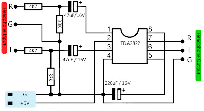
    The circuit is useful to strengthen the voice on the headphones, which is where the headphones have a stereo output is used and paralleled to some headphones. The circuit is based on the TDA2822 amplifier circuit modified to ampifier headphones.


    Amplifier for Paralelling Headphone
    Amplifier for Paralelling Headphone
    In the amplifier circuit I do not put potensio meter to adjust the size of the desired sound on headphones, I just give constraints on two 33K resistors so that the voice issued not too hard. But if you want to make the sound volume settings, you can replace the 33K resistor with potensio meters or trimpot with resistance at 50K. Input voltage in the circuit I took it from a usb DVD, PC, which berkeluaran voltage 5 V DC, which can supply chain so it can work with the good. To parallel his headphones can be seen below...

    Paralel Headphone Wiring Diagram
    Paralel Headphone Wiring Diagram
    Read the rest entry[...]

    Wednesday, March 27, 2013

    DC Coupled Audio Amplifier

    Designs for audio amplifiers with DC coupling to the load are not often encountered these days, even though they offer definite advantages. One advantage is that there is no need for the complication of a second (symmetric) power supply; another is good frequency and phase response. Also, no special electrolytic capacitors are needed for voltage stabilisation, and switch-on ‘thump’ is much reduced. To try to rescue this class of circuit from obscurity the author has designed a headphone amplifier working along the lines illustrated in Figure 1.

    DC-Coupled Audio Amplifier Circuit Diagram


    It consists of a voltage divider, a voltage follower and the loudspeaker in the headphones, whose other side is connected to the junction of two electrolytic capacitors, providing the virtual earth. The potential at this point is, of course, half the supply voltage. All we need to do now is suitably couple in the audio signal to be amplified. Figure 2 shows a practical realisation of this idea in the form of a stereo headphone amplifier. The amplifier itself consists of IC1 and P1, R3 and R4 (giving a gain of 11).

    DC Coupled Audio Amplifier Circuit Diagram


    This part of the circuit demands no further explanation, and the same goes for the voltage divider mentioned above, formed by R1a and R1b. The signal is coupled in via the potentiometers. C2 and R2 have a special purpose: C2 connects the bottom end of the potentiometers (ground for the input signal) to the virtual earth. However, this capacitor creates a feedback path which can lead to oscillation of the amplifier under some circumstances. R2 damps this tendency to oscillate.
    It is possible to calculate suitable values for these components, but it is better to determine them by experiment. C2 must be sufficiently large that stray electric fields do not cause unacceptable hum at the output. R2 must be sufficiently large that the voltage at the amplifier’s virtual earth stabilises quickly enough after switch-on. The polarity of the electrolytic is unimportant as no significant voltage appears across the network. It is possible to try the circuit out with the C2/R2 network shorted and observe the behaviour of the circuit at switch-on using an oscilloscope. Depending on the degree of asymmetry in the circuit, the voltage at the virtual earth point can take a considerable time to stabilise.

    source: http://www.ecircuitslab.com/2011/06/dc-coupled-audio-amplifier.html
    Read the rest entry[...]