Showing posts with label simple. Show all posts

Thursday, January 9, 2014

Simple Bilateral Current Source Circuit Diagram

Hi Friends ! I am sorry for dont update i post because i am busy few days. OK to day share with you Simple Bilateral Current Source Circuit Diagram This circuit uses a CA3193 precision op amp to deliver a current independent of variations in RL. 

With RI set equal to R3, and R2 approximately equal to R4 + R5, the output current, h. is: VlN (R4)/(R3) (R5). 500-I`A load current is constant for load values from 0 to 3ohm.

Simple Bilateral Current Source Circuit Diagram

Simple Bilateral Current Source Circuit Diagram

Read the rest entry[...]

Thursday, December 26, 2013

Simple Gated Alarm

Sometimes the need arises for a simple, gated, pulsed alarm. The circuit shown here employs just four components and a piezo sounder and is unlikely to be out-done for simplicity. While it does not offer the most powerful output, it is likely to be adequate for many applications.

Circuit diagram :
Simple Gated Alarm-Circuit Diagram
Simple Gated Alarm Circuit Diagram
A dual CMOS timer IC type 7556 is used for the purpose, with each of its two halves being wired as a simple astable oscillator (a standard 556 IC will not work in this circuit, nor will two standard 555’s). Note that the CMOS7556 is supplied by many different manufacturers, each using their own type code prefix and suffix. The relevant Texas Instruments product, for instance, will be marked ‘TLC556CN’. The circuit configuration used here is seldom seen, due probably to the inability of this oscillator to be more than lightly loaded without disturbing the timing. However, it is particularly useful for high impedance logic inputs, since it provides a simple means of obtaining a square wave with 1:1 mark-space ratio, which the ‘orthodox’ configuration does not so easily provide.

IC1.A is a slow oscillator which is enabled when reset pin 4 is taken High, and inhibited when it is taken Low. Out-put pin 5 of IC1.A pulses audio oscillator IC1.B, which is similarly enabled when reset pin 10 is taken High, and inhibited when it is taken Low.

In order to simplify oscillator IC1.B, piezo sounder X1 doubles as both timing capacitor and sounder. This is possible because a passive piezo sounder typically has a capacitance of a few tens of nanofarads, although this may vary greatly. As the capacitor-sounder charges and discharges, so a tone is emitted. The value of resistor R2 needs to be selected so as to find the resonant frequency of the piezo sounder, and with this its maximum volume. The circuit will operate off any sup-ply voltage between 2 V and 18 V. A satisfactory output will be obtained at relatively high supply voltages, but do not exceed 18 V.

Author :Rev. Thomas Scarborough –Copyright : Elektor
Read the rest entry[...]

Thursday, October 3, 2013

Simple Remote Control Tester

Nearly always when a remote control doesn’t work, the underlying problem is elementary: the unit does not emit light. The cause may be dry solder joints, defective LEDs etc., but also a flat battery (perhaps due to stuck key). The human eye is unable to perceive infra-red light. By contrast, an ordinary photo transistor like the BP103 has no problems working in the infrared spectrum, so in the circuit here it simply biases the BC558 which, in turn, makes LED D1 flash in sympathy with the telegram from the remote control. The preset in the circuit determines the sensitivity.

Simple Remote Control Tester circuit diagram
Read the rest entry[...]

Thursday, August 15, 2013

Simple Diodeless Rectifier Circuit Diagram

Simple Diodeless Rectifier Circuit Diagram. It`s common knowledge that when working with single-supply op amps, implementing simple functions in a bipolar signal environment can be difficult. Sometimes additional op amps and other electronic components are required. Taking that into consideration, can any advantage be attained from this mode The answer lies in this simple circuit (A). Requiring no diodes, the circuit is a high-precision full-wave rectifier with a liigli-frequency limitation equalling that of the op amps themselves.

 Look at the circuit`s timing diagram (B) to see the principle of operation. The first amplifier rectifies negative input levels with an inverting gain of 2 and turns positive levels to zero.The second amp, a noninverting summing amplifier, adds the inverted negative signal from the first amplifier to the original input signal. The net result is the traditional waveform produced by full-wave rectification. In spite of the limitation on the input signal amplitude (it must be less than VCCJZ), this circuit can be useful in a variety of setups. 

 Diodeless Rectifier Circuit Diagram

Diodeless Rectifier Circuit Diagram
 
Read the rest entry[...]

Friday, August 2, 2013

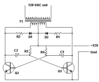
Simple 12 Vdc 120 Vac Inverter Circiut

An Inverter is a device that converts 12 volts d.c to 120 volts a.c. , which is what we use in our homes.  This project will handle about 300 watts, which is perfect for lights, small T.V.s and radio equipment.

This Inverter takes 12 volt d.c  and steps it up to 120 volt a.c.  The wattage depends on which transistors you use for Q1 and Q2, as well as the "Amp Rating" of the transformer you use for T1. This inverter can be constructed to supply anywhere from 1 to 1000 (1 KW) watts. If Q1, Q2 are 2N3055 NPN Transistors and T1 is a 15 A transformer, then the inverter will supply about 300 watts. Larger transformers and more powerful transistors can be substituted for T1, Q1 and Q2 for more power. Note: Dont try to run inductive loads (motors...) off this inverter.

 12 Vdc - 120 Vac Inverter Circuit Diagram

Simple 12 Vdc - 120 Vac Inverter  Circiut

Parts:

C1, C2        68 uf, 25 V Tantalum Capacitor
R1, R2        10 Ohm, 5 Watt Resistor
R3, R4        180 Ohm, 1 Watt Resistor
D1, D2        HEP 154 Silicon Diode
Q1, Q2        2N3055 NPN Transistor (see "Notes")
T1        24V, Center Tapped Transformer
Misc.        Wire, Case, Receptacle (for output)
       Fuses, Heatsinks, etc.


Caution:
This circuit can cause serious injury or death. Keep away from children. Source Link

Read the rest entry[...]

Friday, July 12, 2013

Simple 7805 Voltage Regulator Circuit

A voltage regulator is used to produce a constant linear output voltage. It’s generally used with AC to DC power supply. And also it can be used as well as a DC to DC voltage converter . To regulating low voltage, most used device is one single IC. 7805, 7812, 7905 etc. 78xx series are design for positive and 79xx series are for Negative voltage regulator.

7805 is a three terminal +5v voltage regulator IC from 78XX chips family. See 7805 pinout below. LM78XX series are from National Semiconductor. They are linear positive voltage regulator IC; used to produce a fixed linear stable output voltage.  National Semiconductor has also negative voltage regulator chips family, they indicate with LM 79XX. 78xx is used more than 79xx because negative voltage has a few usability purposes as we see.
I was previously posted a 5v regulated power supply circuit using 7805 IC, that circuit and this 7805 voltage regulator circuit is almost the same.
 
 
Its output voltage is +5V DC that we need. You can supply any voltage in input; the output voltage will be always regulated +5V. But my recommendation is, don’t supply more than 18V or less than 8V in input. There used two capacitors in this voltage regulator circuit, they aren’t mandatory to use. But it will be best if you use them. They helped to produce a smooth regulated voltage at output. Use electrolyte capacitor instead of ceramic capacitor.

One limitation of 7805 I have found that is its output current 1A maximum. Otherwise it is a good voltage regulator if you are happy with 1A. But if   you need over 400mA current in output then you should use a Heat Sink with IC LM7805. Otherwise it may fall damage for overheating.Link
 
Read the rest entry[...]

Tuesday, July 9, 2013

Simple Mini Audio Amplifier circuit

Description

Here is a simple and humble 2 Watts mini audio amplifier circuit suitable for small pocket radios and other portable audio gadgets.The circuit is based on Phillips Semiconductors IC TDA 7052.The amplifier can be run even from a 3V Mercury button cell.This makes it ideal for battery operated gadgets.

The IC TDA7052 is a mono output amplifier coming in a 8-lead DI package (DIP). The device is mainly designed for battery-operated portable audio circuits. The features of TDA 7052 include ,no external components needed,  no switch-on or switch-off click sounds , great overall stability ,very low power consumption(quiescent current 4mA) , low THD, no  heat sinks required and short-circuit proof.

The gain of TDA 7052 is fixed internally at 40 dB. . To compensate the reduction of output power due to low voltage supply  the TDA7052 uses the Bridge-Tied-Load principle (BTL) which can provide  an output  of around 1 to 2 W  Rms(THD = 10%) into an 8 Ohm load with a power supply of 6 V.

In the circuit the potentiometer can be used to control the volume. Capacitor C1 and C2 are meant for  filtering the supply voltage if a battery eliminator is used as supply source. For operations using a battery C1 and C2 are not necessary.

Mini Audio Amplifier Circuit Diagram with Parts List:

mall Audio Amplifier Circuit

Notes.

  • Assemble the circuit on a good quality PCB or common board .
  • If you are a little expert, you can assemble the  circuit in a match box including the speaker.
Read the rest entry[...]

Simple Data accretion System Circuit Diagram

In this circuit, an HA-4900 series comparator is used in conjunction with a D/A converter to form a simple,


Simple Data accretion System Circuit Diagram

versatile, multichannel analog input for a data acquisition system. The processor first sends an address to the D/A, then the processor reads the digital word generated by the comparator outputs, lb perform a simple comparison, the processor sets the D/A to a given reference level, then examines one or more comparator outputs to determine if the inputs are above or below the reference. A window comparison consists of two such cycles with two reference levels set by the D/A. One way to digitize the inputs would be for the processor to increment the D/A in steps. The D/A address, as each comparator switches, is the digitized level of the input. While stairstepping, the D/A is slower than successive approximation; all channels are digitized during one staircase ramp.
Read the rest entry[...]

Sunday, July 7, 2013

Simple Tone Booster Schematic Diagram

This is the tone booster schematic diagram which is published on Everyday Electronics, September 1978 edition. The peaks of frequencies is at 5000 Hz for a “cleaner and more penetrating” sound. The Q1 type is ztx384, while the Q2 is BC415p.

 Simple Tone Booster Schematic Diagram


Read more 

Build a Bass-Treble Tone Control Circuit Diagram

Read the rest entry[...]

Simple Transformerless 5 Volt Power Supply

Description

An increasing number of appliances draw a very small current from the power supply. If you need to design a mains powered device, you could generally choose between a linear and a switch-mode power supply. However, what if the appliance’s total power consumption is very small? Transformer-based power supplies are bulky, while the switchers are generally made to provide greater current output, with a significant increase in complexity, problems involving PCB layout and, inherently, reduced reliability. 

Is it possible to create a simple, minimum part-count mains (230 VAC primary) power supply, without transformers or coils, capable of delivering about 100 mA at, say, 5 V A general approach could be to employ a highly inefficient stabilizer that would rectify AC and, utilizing a zener diode to provide a 5.1 V output, dissipate all the excess from 5.1 V to (230×v2) volts in a resistor. Even if the load would require only about 10 mA, the loss would be approximately 3 watts, so a significant heat dissipation would occur even for such a small power consumption. 

At 100 mA, the useless dissipation would go over 30 W, making this scheme completely unacceptable. Power conversion efficiency is not a major consideration here; instead, the basic problem is how to reduce heavy dissipation and protect the components from burning out. The circuit shown here is one of the simplest ways to achieve the above goals in practice. A JVR varistor is used for overvoltage/surge protection. Voltage divider R1-R2 follows the rectified 230 V and, when it is high enough, T1 turns on and T3 cannot conduct.

Circuit diagram:


When the rectified voltage drops, T1 turns off and T3 starts to conduct current into the reservoir capacitor C1. The interception point (the moment when T1 turns off) is set by P1 (usually set to about 3k3), which controls the total output current capacity of the power supply: reducing P1 makes T1 react later, stopping T3 later, so more current is supplied, but with increased heat dissipation. Components T2, R3 and C2 form a typical ‘soft start’ circuit to reduce current spikes this is necessary in order to limit C1’s charging current when the power supply is initially turned on. At a given setting of P1, the output current through R5 is constant. 

Thus, load R4 takes as much current as it requires, while the rest goes through a zener diode, D5. Knowing the maximum current drawn by the load allows adjusting P1 to such a value as to provide a total current through R5 just 5 to 6 mA over the maximum required by the load. In this way, unnecessary dissipation is much reduced, with zener stabilization function preserved. Zener diode D5 also protects C1 from over voltages, thus enabling te use of low-cost 16 V electrolytics. 

The current flow through R5 and D5, even when the load is disconnected, prevents T3’s gate-source voltage from rising too much and causing damage to device. In addition, T1 need not be a high-voltage transistor, but its current gain should exceed 120 (e.g. BC546B, or even BC547C can be used).

CAUTION!

The circuit is not galvanically isolated from the mains. Touching any part of the circuit (or any circuitry it supplies power to) while in operation, is dangerous and can result in an electric shock! This circuit should not be built or used by individuals without proper knowledge of mains voltage procedures.


Copyright: Elektor Electronics Magazine
Author: Srdjan Jankovic & Branko Milovanovic
Read the rest entry[...]

Saturday, July 6, 2013

Simple 2 1 Surround Speaker System Circuit Diagram

 "Simple 2.1 Surround Speaker System " . Here I have used  three TDA 2030 IC for making signal amplification . Here you need a sub filter extra ( Sub filter circuit diagram link showing below ) . This project  mostly used in computer  . Part list and applications are showing below.

Part List

Component No:ValueUsage
All C1100MF Grounding 
All C2100nFGrounding
All C3100nFGrounding
All C4100MFGrounding
All C5100MFFeedback
All C6100MFAudio Coupling 
All C7220nFNoise Grounding 
All R11K
All R210K ( Not 1K )
All R322K
All R422K (Not 1K )
All RV1100KVolume Controlling 
All D1 To D2IN4007Potential Breaking
U1 To U6TDA2030Amplification

Applications

* 2.1 Surround Amplifier

* 2.1 Home Theater
Read the rest entry[...]

Thursday, April 11, 2013

Simple Smoggy

Even if your good old (Sony) Walkman  sees little use nowadays it would be a  shame to get rid of it altogether. The more  so when just removing the tape head  would allow the built-in audio amplifier  to become an outstanding electrosmog  detector for a variety of purposes. Looking at the schematic, readers with RF  experience will have no difficulty in recognising the diodes and coils of the two  detector-receivers, which serve to capture and demodulate RF signals. With its  coil of four turns (L2) one receiver covers the higher frequency range of the  electromagnetic waves, whilst the sec-ond detector takes care of the lower frequency range.

Simple Smoggy Circuit diagram:
Simple Smoggy-Circuit Schematic

For this reason a coil with a  greater number of turns is required: L1 is  an RF choke of about 250 µH. The precise  value is not critical and it could equally be  220 µH or 330 µH. The outputs of both detector-receivers  are connected to the cables disconnected  previously from the tape heads, feeding the  right and left channel inputs to the Walk-man’s audio amplifier. Please note here that  the screening of the tape head cable does not  have to be absolutely identical to the ground connection of the amplifier circuitry. As  we are dealing with a stereo amplifier,  we are listening into both channels and  thus both RF ranges at the same time.

One channel of the amplifier can also be  used to demodulate low-frequency magnetic alternating fields  via a capacitor  (C3) bypassing diode D1 and connecting either a third coil (L3, for instance;  a telephone recording adapter) as the  pickup device or else a long piece of wire  for acquiring low frequency AC electrical fields. Sources like this are discernible mainly by a distinct 50 Hz (or 60 Hz)  humming in the earphones. Predicting what you may hear down to  the very last detail is difficult, since every  locality has its own, individual interference sources. Nevertheless, with practice  users will succeed in identifying these  interference sources by their particular  audio characteristics.

To sum up, four different ‘sensors’ can be  connected to the inputs of this circuit:  ANT1 (approx. 50 cm long whip antenna),  ANT2 (3.5 cm short stub antenna), ANT3  (approx. 1 m long wire antenna for low frequency electrical fields) and a coil for magnetic fields. Finally, two more tips:
  1. Use only ‘good old’ germanium diodes for  D1 and D2. Sensitivity will be much reduced if  silicon diodes are used, as these have a higher  threshold voltage.
  2. Smoggy does not provide an absolute indi-cation of field strength and even more so can-not provide any guidance whether anything  it detects might be harmful. Its function is to detect electromagnetic signals and compare  their relative magnitude.
Author : Tony Ruepp  - Copyright : Elektor

Source :  http://www.ecircuitslab.com/2012/05/simple-smoggy-circuit-schematic.html
Read the rest entry[...]

Wednesday, April 10, 2013

Simple Mat Switch Circuit

This simple circuit produces a warning beep when somebody crosses a protected area in your home or office. The switch, hidden be-low the floor mat, triggers the alarm when the person walks over it.

The circuit uses a conductive foam as the switch. It can be two small pieces of conductive pads usually used to pack sensitive ICs as antistatic cover. Alternatively, you can make the switch by coating conducting carbon ink on two small pieces of a copper-clad board.

Circuit diagram :

Link


Simple Mat Switch Circuit Diagram

When the circuit is in standby mode, transistor T1 does not conduct, since its base is floating. When the person walks, the switch is pressed and current flows through R1 and the switch to provide positive bias to transistor T1. Transistor T1 conducts and its collector voltage drops, which acts as a negative trigger input for the monostable wired around IC NE555 (IC1).

IC1 outputs a pulse of fifty-seconds duration with preset values of R4 and C3. This pulse is applied to the buzzer through transistor T2. The buzzer sounds a warning beep on unauthorised entry. The pulse duration can be changed to the desired value by changing the values of R4 and C3. Resistor R2 in the circuit makes the trigger pin of IC1 high to prevent false triggering.

Assemble the circuit on a general-purpose PCB and enclose in a plastic case. Use a 9V battery to power the circuit. Connect the touchpad switch with the PCB and hide under the mat at the entrance. The PCB can be mounted on the nearby wall.

Make the switch carefully using conducting foam or copper clad coated with conducting ink. Place the two pieces with their conducting surface facing each other. Solder carefully a thin copper electric wire and ensure that it makes contact when the two plates touch together on pressing. Provide two 1cm rubber tabs between the plates to avoid touch in the standby mode.


http://streampowers.blogspot.com/2012/06/simple-mat-switch-circuit.html 
Read the rest entry[...]

Saturday, April 6, 2013

Ultra Simple Microphone Preamplifier

This little project came about as a result of a design job for a client. One of the items needed was a mic preamp, and the project didnt warrant a design such as the P66 preamp, since it is intended for basic PA only. Since mic preamps are needed by people for all manner of projects, this little board may be just whats needed for interfacing a balanced microphone with PC sound cards or other gear. Unlike most of my boards, this one is double-sided. I normally avoid double-sided PCBs for projects because rework by those inexperienced in working with them will almost certainly damage the board beyond repair. I consider this not to be an issue with this preamp, because it is so simple. It is extremely difficult to make a mistake because of the simplicity.

Ultra-Simple Microphone PreamplifierPhoto of Completed Board

As you can see, the board uses a PCB mounted XLR connector and pot, so is a complete mic preamp, ready to go. Feel free to ignore the terminals marked SW1 (centred between the two electrolytic supply caps), as they are specific to my clients needs and are not useful for most applications. The original use was to use them for a push-button switch that activated an audio switch via a PIC micro-controller. They are not shown on the schematic.

The DC, GND and output terminals may be hard wired to the board, you may use PCB pins or a 10-way IDC (Insulation Displacement Connector) and ribbon cable. Power can be anything between +/-9V and +/-18V with an NE5532 opamp. The mic input is electronically balanced, and noise is quite low if you use the suggested opamp. Gain range is from about 12dB to 37dB as shown. It can be increased by reducing the value of R6, but this should not be necessary. Because anti-log pots are not available, the gain control is not especially linear, but unfortunately in this respect there is almost no alternative and the same problem occurs with all mic preamps using a similar variable gain control system.

Ultra-Simple Microphone Preamplifier circuit diagramFigure 1 - Preamp Schematic

The circuit is quite conventional, and if 1% metal film resistors are used throughout it will have at least 40dB of common mode rejection with worst-case values. The input capacitors give a low frequency rolloff of -3dB at about 104Hz. If better low frequency response is required, these caps may be increased to 4.7uF or 10uF bipolar electrolytics. These will give response to well below 10Hz if you think youll ever need to go that low.

The project PCB measures 77 x 24mm, and the mounting centers for the pot and XLR connector are spaced at 57mm. If preferred, a traditional chassis mounted female XLR can be used, and wired to the board with heavy tinned copper wire. The PCB pads for the connector are in the correct order for a female chassis mount socket mounted with the "Push" tab at the top.
Read the rest entry[...]

Thursday, April 4, 2013

Simple Mat Switch Circuit

This simple circuit produces a warning beep when somebody crosses a protected area in your home or office. The switch, hidden be-low the floor mat, triggers the alarm when the person walks over it.

The circuit uses a conductive foam as the switch. It can be two small pieces of conductive pads usually used to pack sensitive ICs as antistatic cover. Alternatively, you can make the switch by coating conducting carbon ink on two small pieces of a copper-clad board.

Circuit diagram :

Link


Simple Mat Switch Circuit Diagram

When the circuit is in standby mode, transistor T1 does not conduct, since its base is floating. When the person walks, the switch is pressed and current flows through R1 and the switch to provide positive bias to transistor T1. Transistor T1 conducts and its collector voltage drops, which acts as a negative trigger input for the monostable wired around IC NE555 (IC1).

IC1 outputs a pulse of fifty-seconds duration with preset values of R4 and C3. This pulse is applied to the buzzer through transistor T2. The buzzer sounds a warning beep on unauthorised entry. The pulse duration can be changed to the desired value by changing the values of R4 and C3. Resistor R2 in the circuit makes the trigger pin of IC1 high to prevent false triggering.

Assemble the circuit on a general-purpose PCB and enclose in a plastic case. Use a 9V battery to power the circuit. Connect the touchpad switch with the PCB and hide under the mat at the entrance. The PCB can be mounted on the nearby wall.

Make the switch carefully using conducting foam or copper clad coated with conducting ink. Place the two pieces with their conducting surface facing each other. Solder carefully a thin copper electric wire and ensure that it makes contact when the two plates touch together on pressing. Provide two 1cm rubber tabs between the plates to avoid touch in the standby mode.


http://streampowers.blogspot.com/2012/06/simple-mat-switch-circuit.html 
Read the rest entry[...]

Wednesday, April 3, 2013

Simple Automatic Street Light System

The left hand side transistor T1 is rigged as a voltage comparator using a resistive network. The resistor at the upper arm is the LDR and the lower arm resistor is the preset which is used to set the threshold values or levels.  T2 is arranged as an inverter, and inverts the response received from T1.


Initially, assuming the light level is less, the LDR sustains a high resistance level across it, which does not allow enough current to reach the base of the transistor T1. This allows the potential level at the collector to saturate T2 and consequently the relay remains activated in this condition.

When the light level increases and becomes sufficiently large on the LDR, its resistance level falls, this allows more current to pass through it which eventually reaches the base of T1.

The transistor T1 conducts, pulling its collector potential to ground. This inhibits the conduction of the transistor T2, switching OFF its collector load relay and the connected lamp.

The power supply is a standard transformer, bridge, capacitor network, which supplies a clean DC to the circuit for executing the proposed actions.

The whole circuit can be built over a small piece of vero board and the entire assembly along with the power supply may be housed inside a sturdy little plastic box.

 The LDR must be placed outside the box, meaning its sensing surface should be exposed toward the ambient area from where the light level is required to be sensed.

Care should be taken that the light from the lamps does not in any way reach the LDR, which may result in false switching and oscillations.

Parts List

R1, R2, R3 = 2K2,
VR1 = 10K preset,
C1 = 100uF/25V,
C2 = 10uF/25V,
D1 ---- D6 = 1N4007
T1, T2 = BC547,
Relay = 12 volt, 400 Ohm, SPDT,
LDR = any type with 10K to 47K resistance at ambient light.
Transformer = 0-12V, 200m
Read the rest entry[...]