Friday, January 10, 2014
Video Switch for Intercom System


Motor Speed Control

Thursday, January 9, 2014
Intelligent Electronic Lock

Simple Bilateral Current Source Circuit Diagram

Friday, December 27, 2013
Long Range FM Transmitter

- L1 - 4 turns of 20 SWG wire close wound over 8mm diameter plastic former.
- L2 - 2 turns of 24 SWG wire near top end of L1.(Note: No core (i.e. air core) is used for the above coils)
- L3 - 7 turns of 24 SWG wire close wound with 4mm diameter air core.
- L4 - 7 turns of 24 SWG wire-wound on a ferrite bead (as choke)
Thursday, December 26, 2013
Simple Gated Alarm
Circuit diagram :

IC1.A is a slow oscillator which is enabled when reset pin 4 is taken High, and inhibited when it is taken Low. Out-put pin 5 of IC1.A pulses audio oscillator IC1.B, which is similarly enabled when reset pin 10 is taken High, and inhibited when it is taken Low.
In order to simplify oscillator IC1.B, piezo sounder X1 doubles as both timing capacitor and sounder. This is possible because a passive piezo sounder typically has a capacitance of a few tens of nanofarads, although this may vary greatly. As the capacitor-sounder charges and discharges, so a tone is emitted. The value of resistor R2 needs to be selected so as to find the resonant frequency of the piezo sounder, and with this its maximum volume. The circuit will operate off any sup-ply voltage between 2 V and 18 V. A satisfactory output will be obtained at relatively high supply voltages, but do not exceed 18 V.
Wednesday, December 25, 2013
The mutual inspection of cell phone jammer should also be performed
In addition, the rural market is a new market segment, a large number of competitors have not yet entered the competition is not intense, very favorable for Amagatarai phone. Monopolistic tendencies of foreign brands on the channel, so for phones Amagatarai, the key point is to find a breakthrough, in order to build a massive distribution network, the best way is the coexistence of a variety of sales channels. Day language mobile phone retailers, specialty retail, home appliance chain stores, specialized chains and integrated supermarkets, such as shopping malls, supermarkets, etc. should be selected. Different buying habits of consumers, to choose a different retailer, to expand the sales network, to ensure that each class of customers with access to day language phone products. Workshop management of cell phone jammer plays an important role in manufacturing cell phone jammer .cell phone jammer can create enough interference to jam all cell phone signals
To meet the economic characteristics of the contemporary Amagatarai phone channels, the channel length should not be too long, If it is too long, then one for each level distributors to charge some of the profits to the final price of natural variability, is not conducive to the promotion of sales. Flat channel is more conducive to day language is more direct and fast communication with consumers, receive timely feedback information, accurate information on market trends. But the need for a clear channel flat in real terms is the abatement of long and useless links and improve operational efficiency. Constructed between the distributors and consumers of Amagatarai into a complete, organic, and efficient network system. If the worker has any suggestion about workshop management of cell phone jammer , heshe can write a letter to the director.
If the flattening channels of day language to be unrestricted, would like the cost investment in the channel is larger, to centralize power in the distributors, and makes Amagatarai manufacturers in a passive situation. The present tendency of the mobile phone market, the mobile phone hypermarkets position in the market has become increasingly prominent, not only as the Dixon type of specialized cell phone store, and supermarket chains like Gome, Suning, Five Star appliances have also joined. It is due to join supermarkets in the distribution process, the language needs to put in more effort and resources in promoting store sales above. Amagatarai phone should make full use of the advantage of localization and mobile connectivity and other operators to launch a customized mobile phone, meet the diverse needs of consumers. cell phone jammer can create enough interference to jam all cell phone signals.
Tuesday, December 24, 2013
Electric Guitar Preamplifier

Electric Guitar Preamplifier Circuit diagram:

Monday, December 23, 2013
Please inquire any time any nonconforming part of cell phone jammer is found
Wang Lei Leis remarks revealed the "wireless value-added services must rely on win-win" of the mystery. As Chinas leading Internet brands, TOM Onlines focus on the young and trendy demographic, including wireless Internet services and online advertising services. Business scope covers, including SMS, MMS, WAP, wireless interactive services (IVR), content channels, search, classified information, free and paid email services and online games fields. In 2004, TOM Online and the worlds leading instant messaging company Skype co-released multi-TOM-Skype calls for free software. Several cell phone jammer shielding positions will be installed in the whole prison zone.Long currently offers e 230 major cities in China nearly 2,800 hotels and more than 40 000 overseas hotel discount reservation service, domestic more than 50 major business and tourist city out, delivery ticket services, and vacation, group travel, car rental and other travel services. October 2004 e dragon in the U.S. NASDAQ market, the worlds largest online travel company Expedia has a 52% stake in e dragon. Currently, e dragon has become a core part of Expedia Asia, and its in the UK, Canada, Germany, France and other countries, companies, working together to provide consumers with fresh and satisfying travel experience. Today, e dragon work closely with Expedia.
The word is actually simple to do it simple, for the different applications it has different meanings: For an application, you may need a simple installation process, a simple mode of operation; for a website, search engines, users may need to directly address the needs of and not to click time and time again, page after page of the browser. Integration. "Lazy" is the driving force of social development, who can make the user more and more "lazy" will succeed. Integrate it means the user needs to organize information and core functions, for maneuver, showing a lack of cell cell phones, this is even more important. This can be roughly divided into two categories: one is the aggregation of information, but not the accumulation of clutter, but also by integrating the needs of users present, but in fact involves a lot of complicated technology. cell phone jammer intelligent management system is the branch of the wireless information detecting and shielding system.
Another is the integration of functions, which is sought to provide one-stop service - to open the software, looking around the restaurant, find a favorite restaurant scheduled to direct dial the cell phone to receive coupons, easy to use map navigation to cell phones. Shopsavvys success is due to this. Accurate. Accurate integration of the above-mentioned fact, and is one of the integration is the basis of accurate analysis of user needs. Better precision on the one hand to make the user experience, easy access to needed information and applications; the other hand, let advertisers excited, precision will help advertisers target users even more easily accessible to facilitate transactions. LBS, SNS, user behavior analysis and other technologies, will in the future mobile Internet is widely used, a clear picture from all sides of each user, to achieve accurate.
Saturday, December 21, 2013
5V Regulated Power Supply Circuit Diagram
Circuit diagram of 5V Regulated Power Supply
 |
| Fig-1: 5V regulated power supply schematic |
Pin Diagram of IC 7805
 |
| Fig2:Pin Diagram of IC 7805 |
Friday, December 20, 2013
Two Transistor AM Transmitter
Circuit diagram:

Simple AM Transmitter Circuit Diagram
To tune it to a particular frequency, reduce one or both of the 220pF capacitors to raise the frequency or add capacitance in parallel to lower the frequency. Q1 is biased with a 1MO resistor to give a high input impedance and this allows the use of a crystal ear piece as a low cost microphone.
Thursday, December 19, 2013
Song Music generator circuit using ic UM66
Circuit Diagram of Music generator using ic UM66:
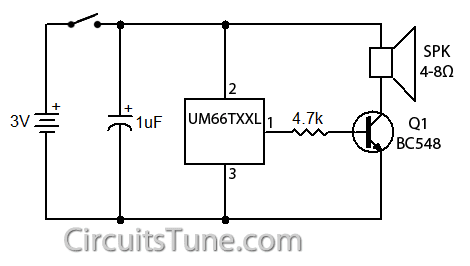 |
| Fig: Circuit Diagram of Song-Music generator using IC-UM66 |
UM66TXX series IC generate different songs-music, the song-music depends on the model of UM66TXX series IC’s. The song-music are listed below with model number.
UM66TXX Songs List:
UM66T01 = Jingle Bells + Santa Claus is coming to town + Wish you a Merry Xmas
UM66T02 = Jingle Bells
UM66T04 = Jingle Bells + Rudolph, the red-nosed reindeer + Joy the world
UM66T05 = Home sweet home
UM66T06 = Let me call you sweetheart
UM66T08 = Happy birthday to you
UM66T09 = Wedding march
UM66T11 = Love me tender, Love me true
UM66T13 = Easter parade
UM66T19 = For Elise
UM66T32 = Waltz
UM66T33 = Mary had a little lamb
UM66T34 = The train is running fast
UM66T68 = Its small world
Wednesday, December 18, 2013
Easy Loudspeaker Circuit For Telephone

- Power rectifier and filter section
This section is made of a simple bridge rectifier and a indicating power LED. - Voltage regulator section
This section is made upon transistor Sl100, which is a general purpose NPN transistor in metal package. That is used to regulate voltage at a level of 9+0.6=9.6V by a 9V zener diode. - Speaker output section
This section contains a high impedance speaker and two BC548 NPN transistor to amplify the signal from line, the input of the 548 transistor pair is fed with a linear or pot control of 10K for volume adjust. - Microphone input section
This section contains a condenser microphone (tablet) and two BC548 NPN transistor to amplify the signal from mic, the output of the 548 transistor pair is fed with a linear or pot control of 10K for volume adjust to the line.
Tuesday, December 17, 2013
Build a Power supply Protection Circuit Diagram
Power supply Protection Circuit Diagram

The trip voltage is set to 5.7 V to protect the equipment in the event of a regulator fault. The 330 ohm resistor and the 500 ohm potentiometer form a potential divider which samples the output voltage as set by adjustment of the potentiometer. The SCR is selected to carry at least twice the fuse rating. The full supply voltage is connected to the input of the regulator.
The 2N2906 is held bias off by the 10 k resistor and the SCR so that the LED is held off. If the output voltage rises above a set trip value then the SCR will conduct, the fuse will blow, and the 2N3906 will be supplied with base current via the 10 k resistor, and the LED will light up.
Wednesday, October 9, 2013
Hi Fi Headphone Amplifier
This design for a headphone amplifier arose after the purchase of commercial equipment with separate pre and power amplifiers without a headphone output.
It is based on designs for a headphone amplifier by John Linsley-Hood, and an active volume control, using a linear pot, by Doug Self (the "pot" circuit was originally designed by P.J. Baxandall), both published in Electronics and Wireless World in recent years.
Its advantages are ...
- is independent of the absolute value of the pot
- has excellent channel tracking
- the O/P noise reduces with gain reduction.
Description
The intention is to permanently insert the headphone amp between pre and power amps, although it can be used as a stand-alone item. The input relay is operated by auxiliary contacts on the headphone sockets through a transistor driver (with a small delay) so as to mute the power amp input when listening on headphones.
The relay contact arrangement enabling it (the headphone amp) to be left switched off when normally not in use. The relay is a high quality, sealed, gold plated contact, TQ signal switching type, reputedly with a very long life expectancy.
The gain control being used to pre-set the gain so that the pre-amps gain control is normally used for setting the listening level.
 Figure 1 - The Headphone Amp Circuit
One channel only is shown, so two units are required for stereo. The gain control pot must be a dual-gang linear type, as the circuit configuration provides the logarithmic law required. This is similar to the circuit shown in Project 01 (except that this version provides a useful reduction of noise). A value of 47k or 100k should be fine in this circuit. Diodes should be 1N4148.
The first stage is a conventional series feedback circuit using the ubiquitous NE5534, the gain being set by the feedback AOT (adjust on test) resistor to suit individual needs, this stage provides the necessary low impedance output for the variable gain stage. The resistor/ capacitor networks around the input stage may seem a little extravagant, but are necessary to reduce any possible RF pickup especially the 470 pF between the two IC + and - inputs.
The complete second stage consists of a zero gain follower, an inverting gain stage and the output emitter followers, volume control gain being set around these three stages. The x10 gain of the inverting stage gives the closest approach to a logarithmic law, stability being ensured by the 27pf capacitor in this stages feedback. The output complementary pair runs in Class-A at about 80 mA and should be mounted on a small heatsink.
Dissipation is about 1.8 Watts for each device, and they must be isolated from the heatsink with mica washers and mounting bushes to prevent short-circuiting the power supply (the collectors are connected to the case). Make sure that heat-conducting paste is used, or use sil-pads for mounting - these require no thermal compound and are very convenient for low power operation.
 Figure 2 - Alternative Relay Driver, and Component Pinouts
The OPA2604 was chosen because its high, FET based, input impedance provides better DC conditions for setting the O/P at 0V DC than the NE5532 alternative, its low output impedance has no problems in driving difficult loads, but it is still relatively cheap.
The power supply is a fairly conventional split variety, the regulated O/Ps feeding the ICs - note the decoupling arrangements - and the 22V pre-regulated supply feeding the O/P transistors, the relay supply being rectified and regulated separately for the necessary isolation, separate signal and supply star earthing being essential

The output jack sockets, with independent changeover contacts, are obtainable from Maplin Electronics and have proved extremely reliable over many years of regular use. If these are not obtainable a circuit is included for use with conventional break contact jack sockets.The LED series resistors will need to supply a current of about 7.5mA, so 2.2k should be used. Diodes for the supply should be 1N4004 or equivalent.
If desired, the 12V regulator may be dispensed with, and suitable value resistors placed in series with each relay coil to retain the correct operating voltage. It is the constructors responsibility to determine the value of these, as the relay current cannot be predicted as there are so many different types available. Use of 15V relays is also possible, if available.
If this arrangement is used, a slight amount of noise may be introduced as the relay operates, because of the sudden application (or removal) of the additional load. It is not expected that this would be a problem in use.
My thanks to Richard for submitting this circuit - it is sure to provide a very high sound quality, and is not overly complex. The active gain control (originally designed by Peter Baxandall) is very effective.
As always, resistors should be 1% metal film types for all signal paths. Their use in the power supply and relay circuits is not necessary, but will not do any harm, either.
Source:www.sound.westhost.com
Tuesday, October 8, 2013
AUDIO SCHEMATIC AND ROUTING ELECTRONIC DIAGRAM

It shows the connection and wiring between each parts and component of audio system of the vehicle such as the alternator, ignition switch, antenna meter, tail, audio, front speaker, rear speaker, tweeter speaker, and many more.
Monday, October 7, 2013
Crowbar Speaker Protection
Crowbar circuits are so-called because their operation is the equivalent of dropping a crowbar (large steel digging implement) across the terminals. It is only ever used as a last resort, and can only be used where the attached circuit is properly fused or incorporates other protective measures.
A crowbar circuit is potentially destructive - if the circuitry only has a minor fault, it will be a major fault by the time a crowbar has done its job. It is not uncommon for the crowbar circuit to be destroyed as well - the purpose is to protect the device(s) attached to the circuit - in this case, a loudspeaker.
Description
Theres really nothing to it. A resistor / capacitor circuit isolates the trigger circuit from normal AC signals. Should there be enough DC to activate the DIAC trigger, the cap is discharged into the gate of the TRIAC, which instantly turns on ... hard. A TRIAC has two basic states, on and off. The in-between state exists, but is so fast that it can be ignored for all intents and purposes.
 Figure 1 - Crowbar Speaker Protector
The BR100 DIAC (or the equivalent DB3 from ST Microelectronics) is rated for a breakdown voltage of between 28 and 36V - these are not precision devices. Needless to say, using the circuit with supply voltages less than around 40V is not recommended, as you will have a false sense of security. The supply voltage must be higher than the breakdown voltage of the DIAC, or it cannot conduct. Zeners cannot be used as a substitute for lower voltages - a DIAC has a negative impedance characteristic, so when it conducts, it will dump almost the full charge in C1 into the gate of the TRIAC. This is essential to make sure the TRIAC is switched into conduction.
The TRIAC is a common type, and may be substituted if you know the specifications. Its rated at 12A, but the peak current (non-repetitive) is 95A, and it only needs to sustain that until the fuse (or an output transistor) blows. A heatsink is preferred, but there is a good chance that the TRIAC will blow up if it has to protect your speakers, so it may not matter too much. The 0.47 ohm resistor is simply to ensure that the short circuit isnt absolute. This will limit the current a little, and increases the chance that the TRIAC will survive (albeit marginally). Feel free to use a BT139 if it makes you feel better - these are rated at 16A continuous, and 140A non-repetitive peak current.
The peak short circuit current will typically be about 90A for a ±60V supply, allowing ~0.2 ohms for wiring resistance and the intrinsic internal resistance of the TRIAC, plus the equivalent series resistance of the filter capacitors. Thats a seriously high current, and it will do an injury to anything thats part of the discharge path. Such high currents are not advised for filter caps either, but being non-repetitive they will almost certainly survive.
Construction & Use
Apart from the obvious requirement that you dont make any mistakes, construction is not critical. Wiring needs to be of a reasonable gauge, and should be tied down with cable ties or similar. C1 must be polyester. While a non-polarised electrolytic would seem to be acceptable, the circuit will operate if the capacitor should dry out over the years. This means it will lose capacitance, and at some point, the crowbar may operate on normal programme material. This would not be good, as it will blow up your amplifier!
Make sure that all connections are secure and well soldered. Remember that this is the last chance for your speakers, so it needs to be able to remain inactive for years and years - hopefully it will never happen. The circuit doesnt have to be mounted in the amplifier chassis - it can be installed in your speaker cabinet. Nothing gets hot unless it operates, at which point no-one really cares - it just has to save the speakers from destruction once to have been worthwhile.
Remember that the crowbar circuit absolutely must never be allowed to operate with any normal signal. A perfectly good amplifier that triggers the circuit because of a high-level bass signal (for example) will very likely be seriously damaged if the crowbar activates. To verify that no signal can trigger it, you may want to (temporarily) use a small lamp in place of R2, and drive the amp to maximum power with bass-heavy material.
A speaker does not need to be connected. If the lamp flashes, your amp would have been damaged. If this occurs, you may want to increase the value of C1. Note that bipolar electrolytics should never be used for C1, because they can dry out and lose capacitance as they age. This could cause the circuit to false-trigger.
Source :www.extremecircuits.net
Sunday, October 6, 2013
METAL DETECTOR USING BEAT FREQUENCY OSCILLATOR ELECTRONIC DIAGRAM

The NAND gates use CMOS 4011 chip, a low power component that is suitable for this battery-operated circuit. You can see that this chip is supplied by a 5V voltage coming from an LM7805L regulator. You might wonder what the purpose of this regulation is, since the power supply come from a 9V battery and the CMOS gates can handle the voltage of 3-15 Volt. The main purpose of the regulator is to keep a constant voltage source for the reference oscillator frequency stability, since the frequency is affected by the power supply voltage variation as the battery voltage drops in the long time of usage.
This circuit uses parts as follows :
- U1: CD4011
- U2: LM389
- U3: 78L05
- R1: 2.2k 5%
- P2: 4.7k lin.
- R3: 330k 5%
- R4: 270k 5%
- R5: 1k 5%
- C1: 390pF (NPO)
- C2,C3,C4: 10nF
- C5: 10uF 16v electrolytic
- C6,C8: 220 uF 16v electrolytic
- C7: 100uf 16v electrolytic
- C9: 100nF ceramic
- P1: 4.7k log
- L1: 22cm in diameter with 14 turns AWG 26
- K1: SPDT toggle switch
- J1= Headphone jack 1/4 or 1/8 inch
- Other parts: 9v battery connector, speaker or headphones
Saturday, October 5, 2013
Baud Rate Generator
In this article, an RC oscillator is used as a baud rate generator. If you can calibrate the frequency of such a circuit sufficiently accurately (within a few percent) using a frequency meter, it will work very well. However, it may well drift a bit after some time, and then…. Consequently, here we present a small crystal-controlled oscillator. If you start with a crystal frequency of 2.45765 MHz and divide it by multiples of 2, you can very nicely obtain the well-known baud rates of 9600, 4800, 2400, 600, 300, 150 and 75. If you look closely at this series, you will see that 1200 baud is missing, since divider in the 4060 has no Q10 output!

If you do not need 1200 baud, this is not a problem. However, seeing that 1200 baud is used in practice more often than 600 baud, we have put a divide-by-two stage in the circuit after the 4060, in the form of a 74HC74 flip-flop. This yields a similar series of baud rates, in which 600 baud is missing. The trimmer is for the calibration purists; a 33 pF capacitor will usually provide sufficient accuracy. The current consumption of this circuit is very low (around 1mA), thanks to the use of CMOS components.
Friday, October 4, 2013
High Side Current Measurements
This current can be used directly, or it can be converted into a voltage by means of a load resistor RL. In the latter case, the ‘floating’ measurement voltage across the shunt is converted into a voltage with respect to earth, which is easy to use. The value of RL determines the gain. A value of 5 kΩ gives 1×, 10 kΩ gives 2×, 15 kΩ gives 3× and so on. It all works as follows. Just like any opamp, this IC tries to maintain the same potential on its internal plus and minus inputs. The minus input is connected to the left-hand end of the shunt resistor via a 5-kΩ resistor.
 When a current flows through the shunt, this voltage is thus lower than the voltage on the plus side. However, the voltage on the plus input can be reduced by allowing a small supplementary current to flow through T1. The IC thus allows T1 to conduct just enough to achieve the necessary lower voltage on the plus input. The current that is needed for this is equal to Vshunt / 5 kΩ. This transistor current leaves the IC via the output to which RL is connected. If the value of RL is 5 kΩ, the resulting voltage is exactly the same as Vshunt. The IC is available in two versions.
The INA138 can handle voltages between 2.7 and 36 V, while the INA168 can work up to 60 V. The supply voltage on pin 5 may lie anywhere between these limits, regardless of the voltage on the inputs. This means that even with a supply voltage of only 5 V, you can make measurements with up to 60 V on the inputs! However, in most cases it is simplest to connect pin 5 directly to the voltage on pin 3. Bear in mind that the value of the supply voltage determines the maximum value of the output voltage. Also, don’t forget the internal base-emitter junction voltage of T1 (0.7 V), and the voltage drop across the shunt also has to be subtracted.