Wednesday, July 31, 2013

2005 3 5l Chevrolet Colorado Wiring Harness Diagram


The following schematic shows the 2005 3.5l Chevrolet Colorado Wiring Harness Diagram. This is a car powered by a straight, five cylinders engine or inline-five engine with 3.5L (3,460 cc/211 cu in) total displacement. The bore is 93 mm (3.7 in) and the stroke is 102 mm (4.0 in), this is a straight-five truck engine called the Vortec 350. It has long stroke (the stroke is longer than the bore) for better torque. (click image to enlarge)


LEGEND for the 2005 3.5l Chevrolet Colorado Wiring Harness Diagram:
(1) Accessory Switch C2
(2) Hazard Switch
(3) Accessory Switch C1
(4) Digital Radio Receiver (U2K)
(5) Inflatable Restraint I/P Module
(6) Ambient Light Sensor
(7) Vehicle Communication Interface Module (VCIM) (UE1)
(8) Courtesy Lamp – Footwell Right
(9) Body Control Module (BCM) C2
(10) C201 (I/P Harness to Body Harness)
(11) HVAC Control Module C1
(12) Auxiliary Power Outlet 2
(13) Auxiliary Power Outlet 1
(14) HVAC Control Module C2
(15) Courtesy Lamp – Footwell Left
(16) Data Link Connector (DLC)
(17) C204 (Steering Column Harness to I/P Harness)
(18) C208 (I/P Harness to Body Harness)
(19) C200 (I/P Harness to Body Harness)
(20) Headlamp and Panel Dimmer Switch
(21) Instrument Panel Cluster (IPC)
(22) Radio C1
(23) Radio C2
Read the rest entry[...]

Tuesday, July 30, 2013

4 Bit Analogue to Digital Converter

The operation of the converter is based on the weighted adding and transferring of the analogue input levels and the digital output levels. It consists of comparators and resistors. In theory, the number of bits is unlimited, but each bit needs a comparator and several coupling resistors. The diagram shows a 4-bit version. The value of the resistors must meet the following criteria:
  • R1:R2 = 1:2;
  • R3:R4:R5 = 1:2:4;
  • R6:R7:R8:R9 = 1:2:4:8.
The linearity of the converter depends on the degree of precision of the value of the resistors with respect to the resolution of the converter, and on the accuracy of the threshold voltage of the comparators. This threshold level must be equal, or nearly so, to half the supply voltage. Moreover, the comparators must have as low an output resistance as possible and as high an input resistance with respect to the load resistors as feasible. Any deviation from these requirements affects the linearity of the converter adversely.
Circuit diagram:
4-bit_AnalogueTo_Digital_Converter-Circuit-Diagramw
4-Bit Analogue to Digital Converter Circuit Diagram
If the value of the resistors is not too low, the use of inverters with an FET (field-effect transistor) input leads to a near-ideal situation. In the present converter, complementary metal-oxide semiconductor (CMOS) inverters are used, which, in spite of their low gain, give a reasonably good performance. If standard comparators are used, take into account the output voltage range and make sure that the potential at their non-inverting inputs is set to half the supply voltage. If high accuracy is a must, comparators Type TLC3074 or similar should be used. This type has a totem-pole output. The non-inverting inputs should be interlinked and connected to the tap of a a divider consisting of two 10 kΩ resistors across the supply lines. It is essential that the converter is driven by a low-resistance source. If necessary, this can be arranged via a suitable op amp input buffer. The converter draws a current not exceeding 5 mA.
Source :www.extremecircuits.net
Read the rest entry[...]

Monday, July 29, 2013

Insulation Resistance Measurement of an installation to Ground

                    
-> The installation, power off the
-> Make sure that lamps remain switched on for all recipients, including
-> It turned out that one end of the ground, connect the other end of the one-energized conductors installation
-> If you switch the button to turn on the meter
-> Read the value of the display by turning the lever Magneto
-> We read the value of the insulation resistance to earth of installation.
Read the rest entry[...]

Friday, July 26, 2013

Build a Carrier Operated Relay Circuit Diagram

Carrier-Operated Relay Circuit Diagram shows a COR/CAS circuit for repeater use. CR1 is a silicon diode. 2 may be any relay with a 12-V coil (a long-life-reed relay is best). R2 sets the length of time that K2 remains closed after the input voltage disappears (hang time). shows a timer circuit. Values shown for Rl and CI should provide timing up to four minutes or so. CI should be a low-leakage capacitor; Ql is a silicon-controlled rectifier, ECG-5452 or equivalent. 

Kl may be any miniature relay with a 12-volt coil. The timer is reset when the supply voltage is momentarily interrupted. The switch must be in the reset position for the remote reset to work. This circuit operates from the detector output of a receiver. A delay circuit is included so that the relay stays closed for a time period after the carrier output from the receiver disappears. 

  Carrier-Operated Relay Circuit Diagram

 Carrier-Operated Relay Circuit Diagram
 
Read the rest entry[...]

Saturday, July 13, 2013

LA4440 Bridge Amplifier Circuit Diagram

LA4440 is a dual channel audio amplifier IC. It can be used in two modes; one is Stereo amplifier and another Bridge amplifier mode. The LA4440 is a monolithic linear IC from Sanyo. Here I give the both circuit mode of amplifier using IC LA4440.

When the IC LA4440 is in Bridge mode in the circuit, its output power is 19w. In bridge mode use 4Ω-8Ω speaker. If you want stereo output(19w+19w) in bridge mode then use two copies of amplifier circuit of given below. Resistor R3&R4 is to adjust the voltage gain and for making input signal of inverting amplifier.

LA4440 Bridge Amplifier Circuit Diagram

C10 is filter capacitor used to reduce the ripple of supply voltage. Don’t decrease the value of capacitor C6&C7 less than 100uF, 10v, it may causes of the output at low frequencies goes lower. The pin-6 of LA4440 amplifier circuit  is audio input pin; it used in stereo amplifier mode but in bridge mode it is grounded. C8&C9 are polyester film capacitor used to preventing oscillation, and R1&R2 used for the same reason as filter resistor. Though the maximum supply voltage for both circuit of amplifier is 18V but we recommend to use a 12V,3A power supply. Use a good quality heat sink with LA4440.

I think here you see little comparison between stereo and bridge amplifier of LA4440. If you want to make this amplifier project, then I recommend you the bridge one. I think it is ideal for a beginner. And I love its wattage rather than Stereo mode. There is also a possibilities as I say, make two copies of circuit of bridge amplifier for stereo, it will give you 19w+19w of audio power output.
Read the rest entry[...]

Intelligent Presence Simulator

However effective a domestic alarm system may be, it’s invariably better if it never goes off, and the best way to ensure this is to make potential burglars think the premises are occupied. Indeed, unless you own old masters or objects of great value likely to attract ‘professional’ burglars, it has to be acknowledged that the majority of burglaries are committed by ‘petty’ thieves who are going to be looking more than anything else for simplicity and will prefer to break into homes whose occupants are away.

Rather than simply not going on holiday – which is also one solution to the problem (!) – we’re going to suggest building this intelligent presence simulator which ought to put potential burglars off, even if your home is subjected to close scrutiny. Like all its counterparts, the proposed circuit turns one or more lights on and off when the ambient light falls, but while many devices are content to generate fixed timings, this one works using randomly variable durations.

Circuit diagram:
 intelligent-presence-simulator-circuit-diagramw
Intelligent Presence Simulator Circuit Diagram

So while other devices are very soon caught out simply by daily observation (often from a car) because of their too-perfect regularity, this one is much more credible due to the fact that its operating times are irregular. The circuit is very simple, as we have employed a microcontroller – a ‘little’ 12C508 from Microchip, which is more than adequate for such an application. It is mains powered and uses rudimentary voltage regulation by a zener diode.


A relay is used to control the light(s); though this is less elegant than a triac solution, it does avoid any interference from the mains reaching the microcontroller, for example, during thunderstorms. We mustn’t forget this project needs to work very reliably during our absence, whatever happens. The ambient light level is measured by a conventional LDR (light dependent resistor), and the lighting switching threshold is adjustable via P1 to suit the characteristics and positioning of the LDR.

Note that input GP4 of the PIC12C508 is not analogue, but its logic switching threshold is very suitable for this kind of use. The LED connected to GP1 indicates the circuit’s operating mode, selected by grounding or not of GP2 or GP3 via override switch S1. So there are three possible states: permanently off, permanently on, and automatic mode, which is the one normally used. Given the software programmed into the 12C508 (‘firmware’) and the need to generate very long delays so as to arrive at lighting times or an hour or more, it has been necessary to make the MCU operate at a vastly reduced clock frequency.

PCB Layout:
pcb-layout-of-intelligent-presence-sim
PCB Layout Of Intelligent Presence Simulator

In that case, a crystal-controlled clock is no longer suitable, so the R-C network R5/C3 is used instead. For sure, such a clock source is less stable than a crystal, but then in an application like this, that may well be what we’re after as a degree of randomness is a design target instead of a disadvantage. Our suggested PCB shown here takes all the components for this project except of course for S1, S2, and the LDR, which will need to be positioned on the front panel of the case in order to sense the ambient light intensity.

The PCB has been designed for a Finder relay capable of switching 10 A, which ought to prove adequate for lighting your home, unless you live in a replica of the Palace of Versailles. The program to be loaded into the 12C508 is available for free download from the Elektor website as file number 080231-11.zip or from the author’s own website: www.tavernier-c.com. On completion of the solder work the circuit should work immediately and can be checked by switching to manual mode.

The relay should be released in the ‘off’ position and energized in the ‘on’ position. Then all that remains is to adjust the day/night threshold by adjusting potentiometer P1. To do this, you can either use a lot of patience, or else use a voltmeter – digital or analogue, but the latter will need to be electronic so as to be high impedance – connected between GP4 and ground. When the light level below which you want the lighting to be allowed to come on is reached, adjust P1 to read approximately 1.4 V on the voltmeter.

If this value cannot be achieved, owing to the characteristics of your LDR, reduce or increase R8 if necessary to achieve it (LDRs are known to have rather wide production tolerances). Equipped with this inexpensive accessory, your home of course hasn’t become an impregnable fortress, but at least it ought to appear less attractive to burglars than houses that are plunged into darkness for long periods of time, especially in the middle of summer. (www.tavernier-c.com)

COMPONENTS LIST Resistors
R1 = 1k 500mW
R2 = 4k7
R3 = 560R
R4,R6 = 10k
R5 = 7k5
R 7 = LDR
R8 = 470k to 1 M
P1 = 470k potentiometer
Capacitors
C1 = 470µF 25V
C2 = 10µF 25V
C3 = 1nF5
C4 = 10nF
Semiconductors
D1,D2 = 1N4004
D3 = diode zener 4V7 400 mW
LED1 = LED, red
D4 = 1N4148
T1 = BC547
IC1 = PIC12C508, programmed, see Downloads
Miscellaneous
RE1 = relay, 10A contact
S1 = 1-pole 3-way rotary switch
F1 = fuse 100 mA
TR1 = Mains transformer 2x9 V, 1.2 -3 VA
4 PCB terminal blocks, 5 mm lead pitch
5 solder pins 


www.ecircuitslab.com
Read the rest entry[...]

Two Band Radio Schematic

This TRF receiver covers the AM broadcast, band and longwave bands (used in Europe and Asia for broadcasting). A loop antenna is used for reception and an external antenna can be connected. Frequency coverage is 150 to 1600 kHz.

Two-Band Radio Circuit Diagram


Read the rest entry[...]

Friday, July 12, 2013

On Demand WC Fan Using 555

In most WCs with an extractor the fan is connected to the lighting circuit and is switched on and off either in sympathy with the light or with a short delay. Since toilets are sometimes used for washing the hands or just for a quick look in the mirror, it is not always necessary to change the air in the smallest room in the house. The following circuit automatically determines whether there really is any need to run the fan and reacts appropriately. No odour sensor is needed: we just employ a small contact that detects when and for how long the toilet seat lid is lifted.

If the seat lid is left up for at least some presettable minimum time t1, the fan is set running for another presettable time t2. In the example shown the contact is made using a small magnet on the lid and a reed switch mounted on the cistern. The rest is straightforward: IC2, the familiar 555, forms a timer whose period can be adjusted up to approximately 10 to 12 minutes using P2. This determines the fan running time. There are three CMOS NAND gates (type 4093) between the reed switch and the timer input which generate the required trigger signal. When the lid is in the ‘up’ position the reed switch is closed.

On-Demand WC FanCapacitor C1 charges through P1 until it reaches the point where the output of IC1a switches from logic 1 to logic 0. The output of IC1b then goes to logic 1. The edge of the 0-1 transition, passed through the RC network formed by C2 and R2, results in the output of IC1c going to logic 0 for a second. This is taken to the trigger input on pin 2 of timer IC2, which in turn switches on the relay which causes the fan to run for the period of time determined by P2. The circuit is powered from a small transformer with a secondary winding delivering between approximately 8 V and 10 V. Do not forget to include a suitable fuse on the primary side.

The circuit around IC1b and IC1c ensures that the fan does not run continuously if the toilet seat lid is left up for an extended period. The time constant of P1 and C1 is set so that the fan does not run as a result of lavatorial transactions of a more minor nature, where the lid is opened and then closed shortly afterwards, before C1 has a chance to charge sufficiently to trigger the circuit.


Circuit Source: DIY Electronics Projects
Read the rest entry[...]

100W Guitar Pre Amplifier Rise

Introduction
Guitar amplifiers are always an fascinating challenge. The tone controls, gain & overload characteristics are individual, & the ideal combination varies from guitarist to the next, & from guitar to the next. There is no amp that satisfies everyones requirements, & this offering is not expected to be an exception. The preamp is now at Revision-A, & although the whole schematic of the new version is not shown below, the essential characteristics are not changed - it still has the same tone control "stack" & other controls, but now has a second op amp to reduce output impedance & improve gain characteristics.

One major difference from any "store bought" amplifier is that in case you build it yourself, you can alter things to fit your own needs. The ability to experiment is the key to this circuit, which is although introduced in complete form, there is every expectation that builders will make modifications to suit themselves.

The amp is rated at 100W in to a four Ohms load, as this is typical of a "combo" type amp with 8 Ohm speakers in parallel. Alternatively, you can run the amp in to a "quad" box (four x 8 Ohm speakers in series parallel - see Figure five in Project 27b, the original editorial) and will get about 60 Watts. For the adventurous, two quad boxes and the amp head will provide 100W, but will be much louder than the twin. This is a common combination for guitarists, but it does make it hard for the sound man to bring everything else up to the same level.

The Pre-Amplifier
A picture of the Revision-A preamp is shown below. Youll see that theres dual op amps, but the schematic only shows. This is the main part of the Rev-A update - the output section now has gain (which is basically selected), and a better buffered low output impedance. The remainder of the circuit is unchanged.

Guitar Pre-Amplifier Board

The preamp circuit is shown in Figure one, and has a few fascinating characteristics that separate it from the "normal" - assuming that there is such a thing. This is simple but elegant design, that provides excellent tonal range. The gain structure is designed to provide a immense amount of gain, which is ideal for those guitarists who like to get that fully distorted "fat" sound.

However, with a couple of simple changes, the preamp can be tamed to suit any style of playing. Likewise, the tone controls as shown have sufficient range to cover very anything from an electrified violin to a bass guitar - The response can be limited in the event you wish (by experimenting with the tone control capacitor values), but I recommend that you try it "as is" before making any changes.

Figure 1 - Guitar Pre-Amplifier

From Figure one, you can see that the preamp makes use of a dual op amp as its only amplification. The lone transistor is an emitter follower, & maintains a low output impedance after the master volume control. As shown, with a typical guitar input, it is feasible to receive a fat overdrive sound by winding up the volume, & then setting the master for an appropriate level. The general frequency response is deliberately limited to prevent extreme low-end waffle, & to cut the extreme highs to help reduce noise & to limit the response to the normal requirements for guitar. In case you use the TL072 op amp as shown, you may find that noise is an issue - at high gain with lots of treble boost. I strongly recommend that you use an OPA2134 - a premium audio op amp from Los angels Instruments (Burr-Brown division), you will then find this possibly the quietest guitar amp you have ever heard (or not heard :-). At any gain setting, there is more pickup noise from my guitar than circuit noise - & for the prototype one used carbon resistors!

Notes:
one - IC pin outs are industry standard for dual op amps - pin four is -ve supply, and pin 8 is +ve supply.
two - Op amp supply pins must be bypassed to earth with 100nF caps (preferably ceramic) as close as feasible to the op amp itself.
three - Diodes are 1N4148, 1N914 or similar.
four - Pots ought to be linear for tone controls, & log for volume and master.

The power supply section (bottom left corner) connects directly to the main +/-35V power amp supply. Use one Watt zen-er diodes (D5 and D6), and make positive that the zen-er supply resistors (R18 and R19, 680 ohm one Watt) are kept away from other parts, as they will get warm in operation. Again, the preamp PCB accommodates the supply on the board.

The pin connections shown (either huge dots or "port" symbols) are the pins from the PCB. Normally, all pots would be PCB types, and mounted directly to the board. For a do-it-yourself project, that would limit the layout to that imposed by the board, so all connections use wiring. It may look a bit hard, but is simple and looks fine when the unit is done. Cable ties keep the wiring tidy, and only a single connection to the GND point ought to be used(several are provided, so select that suits your layout. VCC is +35V from the main supply, and VEE is the -35V supply.

In the event you dont require all the gain that is available, basically increase the worth of R6 (the first 4k7 resistor) - for even less noise and gain, increase R11 (the second 4k7) as well. For more gain, decrease R11 - I recommend a maximum of 2k2 here.


If the bright switch is bright ( much treble), increase the 1k resistor (R5) to tame it down again. Reduce the worth to get more bite. The tone control arrangement shown will give zero output if all controls are set to maximum - this is unlikely to be a common requirement in use, but be aware of it when testing.

The diode network at the output is designed to permit the preamp to generate a "soft" clipping characteristic when the volume is turned up. Because of the diode clipping, the power amp needs to have an input sensitivity of about 750mV for full output, otherwise it wont be feasible to get full power even with the Master gain control at the maximum setting.

Make positive that the input connectors are isolated from the chassis. The earth isolation parts in the power supply help to prevent hum ( when the amp is connected to other mains powered equipment).
If issues are encountered with this circuit, then you have made a wiring mistake .. period. A golden rule here is to check the wiring, then keep on checking it until you find the error, since I can assure you that if it does not work properly there is at least mistake, & probably more.


The input, effects & output connections are shown in Figure 1B.

Figure 1B - Internal Wiring

The connections shown are similar (ok, virtually identical :-) to those used in my prototype. Noise is low, & probably might have been lower if I had made the amp a tiny bigger. All connectors must be fully insulated types, so there is no connection to chassis. This is important !

You will notice from the above diagram that I didnt include the "loop breaker" circuit shown in the power supply diagram. For my needs, it is not necessary, for your needs, I shall let you pick. In case you select to make use of it, then the earth (chassis) connection marked * (next to the input connectors) must be left off.

A few important points
The main 0 volt point is the connection between the filter caps. This is the reference for all zero volt returns, including the 0.1 ohm speaker feedback resistor. Dont connect the feedback resistor directly to the amps GND point, or you will generate distortion & feasible instability.
 The supply for the amp & preamp must be taken directly from the filter caps - the diagram above is literal - that means that you follow the path of the wiring as shown.
 Although mentioned above, you might well ask why the pots dont mount directly to the PCB to save wiring. Simple . Had I done it that way, you would require to make use of the same type pots as I designed for, & the panel layout would must be the same , with the exact same spacings. I figured that this would be limiting, so wiring it is. The wiring actually doesnt take long & is simple to do, so is not an issue.
 I didnt include the "Bright" switch in Figure 1B for clarity. I expect that it will cause few issues.


Read the rest entry[...]

Simple 7805 Voltage Regulator Circuit

A voltage regulator is used to produce a constant linear output voltage. It’s generally used with AC to DC power supply. And also it can be used as well as a DC to DC voltage converter . To regulating low voltage, most used device is one single IC. 7805, 7812, 7905 etc. 78xx series are design for positive and 79xx series are for Negative voltage regulator.

7805 is a three terminal +5v voltage regulator IC from 78XX chips family. See 7805 pinout below. LM78XX series are from National Semiconductor. They are linear positive voltage regulator IC; used to produce a fixed linear stable output voltage.  National Semiconductor has also negative voltage regulator chips family, they indicate with LM 79XX. 78xx is used more than 79xx because negative voltage has a few usability purposes as we see.
I was previously posted a 5v regulated power supply circuit using 7805 IC, that circuit and this 7805 voltage regulator circuit is almost the same.
 
 
Its output voltage is +5V DC that we need. You can supply any voltage in input; the output voltage will be always regulated +5V. But my recommendation is, don’t supply more than 18V or less than 8V in input. There used two capacitors in this voltage regulator circuit, they aren’t mandatory to use. But it will be best if you use them. They helped to produce a smooth regulated voltage at output. Use electrolyte capacitor instead of ceramic capacitor.

One limitation of 7805 I have found that is its output current 1A maximum. Otherwise it is a good voltage regulator if you are happy with 1A. But if   you need over 400mA current in output then you should use a Heat Sink with IC LM7805. Otherwise it may fall damage for overheating.Link
 
Read the rest entry[...]

Auto Turn Off Alarm With 8 Minute Delay

This circuit uses a NE555 timer and CD4020B. When +12 Vdc is applied to the circuit, the output of IC2 is set low via C2, which turns on the relay, and IC1, a pulse generator.

Auto Turn-Off Alarm With 8-Minute Delay Circuit Schematic

Automotive Circuit Diagram
IC1 pulses counter IC2. After 8192 clocks, IC2 output (pin 3) goes high, cuts off Q2, and completes the cycle.

Read the rest entry[...]

Thursday, July 11, 2013

Battery Discharger Using Discrete Components

The battery discharger published in this website may be improved by adding a Schottky diode (D3). This ensures that a NiCd cell is discharged not to 0.6–0.7 V, but to just under 1 V as recommended by the manufacturers. An additional effect is then that light-emitting diode D2 flashes when the battery connected to the terminals is flat. The circuit in the diagram is based on an astable multivibrator operating at a frequency of about 25 kHz. When transistor T2 conducts, a current flows through inductor L1, whereupon energy is stored in the resulting electromagnetic field. When T2 is cut off, the field collapses, whereupon a counter-emf is produced at a level that exceeds the forward voltage (about 1.6 V) of D2.

Battery Discharger Circuit Diagram0

A current then flows through the diode so that this lights. Diode D1 prevents the current flowing through R4 and C2. This process is halted only when the battery voltage no longer provides a sufficient base potential for the transistors. In the original circuit, this happened at about 0.65 V. The addition of the forward bias of D3 (about 0.3 V), the final discharge voltage of the battery is raised to 0.9–1.0 V. Additional resistors R5 and R6 ensure that sufficient current flows through D3. When the battery is discharged to the recommended level, it must be removed from the discharger since, in contrast to the original circuit, a small current continues to flow through D3, R2-R3, and R5-R6 until the battery is totally discharged.

The flashing of D2 when the battery is nearing recommended discharge is caused by the increasing internal resistance of the battery lowering the terminal voltage to below the threshold level. If no current flows, the internal resistance is of no consequence since the terminal voltage rises to the threshold voltage by taking some energy from the battery. When the discharge is complete to the recommended level, the LED goes out. It should therefore be noted that the battery is discharged sufficiently when the LED begins to flash.
 
 
Streampowers
Read the rest entry[...]

Coil Coupled Operation Metal Detector

A Coil Coupled Operation Metal Detector made from readily obtainable components and using an ordinary medium receiver as a detector.

Coil Coupled Operation Metal Detector Circuit Diagram


Notes:

The metal detector shown here may well represent a new genre. At any rate, after some exposure, it is regarded as such by those who have seen it. It is based on a standard transformer coupled oscillator (TCO)  hence the name Coil Coupled Operation (CCO) Metal Detector. Although requiring a BFO (in this case provided by a Medium Wave radio), it differs from a typical BFO detector in that its performance far outstrips that of BFO. Also, unlike BFO, it is dependent on the balance of two coils to boost sensitivity. It also differs from IB, in that its Rx section is an active, rather than passive, component of the oscillator. Further, unlike IB, the design does not require critical placement of the coils. As with both BFO and IB, the design provides discrimination. Experiments with different embodiments of the idea have shown that it has the potential to match the best of IB. Happy hunting!
Read the rest entry[...]

Sound Operated Switch

This sensitive sound operated switch can be used with a dynamic microphone insert as above, or be used with an electret (ECM) microphone. If an ECM is used then R1 (shown dotted) will need to be included. A suitable value would be between 2.2k and 10kohms.

Sound Operated Switch Circuit diagram


The two BC109C transitors form an audio preamp, the gain of which is controlled by the 10k preset.  The output is further amplified by a BC182B transistor. To prevent instability the preamp is decoupled with a 100u capacitor and 1k resistor. The audio voltage at the collector of the BC182B is rectified by the two 1N4148 diodes and 4.7u capacitor. This dc voltage will directly drive the BC212B transistor and operate the relay and LED.

It should be noted that this circuit does not "latch". The relay and LED operate momentarily in response to audio peaks.
Read the rest entry[...]

Variable 5 to 20V DC Supply Rise

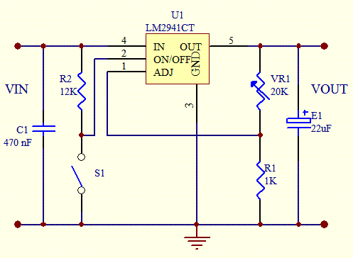
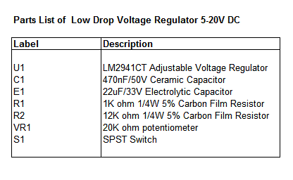
If you are looking for a low drop voltage regulator that can provide a power supply of 1A with an output voltage of between 5V and 20V DC, National Semiconductor LM2941 Low Dropout Adjustable Regulator is that you can pick to make use of. Its a typical dropout voltage of 0.5V which means that the input supply need only must be 0.5V DC over the desired output voltage. Its other features include internal short circuit current limit and reverse battery protection.

As shown in the schematic below, the regulator has five pins which consists of the ON/OFF control, Input Voltage, Output Voltage, Ground & Adjustable pins. ON/OFF is used for the purpose of switching on & off of the regulator. The capacitors C1 & E1 are to be placed as close as feasible to the regulator.


The output of the circuit can be varied by varying the worth of potentiometer VR1 from 5V DC to 20V DC. The input voltage is limited from five.5V DC to 30V DC. Resistor R1 must be greater than 1K. The worth of the VR1 that needs to be set is calculated from the formula given below:

VR1 = R1[(Vout/1.275) - 1] ohm

If R1=1K, Vout = 5V, VR1 should be set to 2.9K ohm.

If R1=1K, Vout = 20V, VR1 should be set to 14.7K ohm

Read the rest entry[...]

Wednesday, July 10, 2013

RGB Solar Lamp

This deluxe solar-powered light  uses a battery and solar cells salvaged from a solar lamp with a four-cell battery (4.8 V nominal terminal  voltage).
Circuit diagram :
RGB Solar Lamp-Circuit Diagram
RGB Solar Lamp Circuit Diagram

The circuit can operate from any  DC voltage around this value and  its current consumption, at 20 mA,  is low. This means that the battery  can give up to five days of operation. The circuit consists of an Atmel  ATtiny microcontroller which drives  a red, a green and a blue LED directly  from three port pins. Series resistors are of course included to limit  the LED current. The microcontroller  drives the LEDs in sequence to produce an  RGB running light effect. The microcontroller  is also responsible for ensuring that the light automatically switches on when it gets dark  and off when it is light. The light sensor is  made from one of the solar cells from a bro-ken solar lamp (it is more common  for the battery to fail rather than  the solar cells). 

The power output of this cell is not  important, as the microcontroller  only measures its output voltage  using its internal A/D converter  connected to pin PB4. The project is  ideal for beginners, as a ready-programmed microcontroller is avail-able from the Elektor Shop (order  code 100581-41). 


Source by : Streampowers
Read the rest entry[...]

Automatic Night Lamp with Morning Alarm

This circuit automatically turns on a night lamp when bedroom light is switched off. The lamp remains ‘on’ until the light sensor senses daylight in the morning. A super-bright white LED is used as the night lamp. It gives bright and cool light in the room. When the sensor detects the daylight in the morning, a melodious morning alarm sounds. The circuit is powered from a standard 0-9V transformer. Diodes D1 through D4 rectify the AC voltage and the resulting DC voltage is smoothed by C1. Regulator IC 7806 gives regulated 6V DC to the circuit. A battery backup is provided to power the circuit when mains fails. When mains supply is available, the 9V rechargeable battery charges via diode D5 and resistor R1 with a reasonably constant current. In the event of mains failure, the battery automatically takes up the load without any delay. Diode D5 prevents the battery from discharging backwards following the mains failure and diode D6 provides current path from the battery. 

Circuit diagram :
Automatic Night Lamp with Morning Alarm-Circuit-Diagram
Automatic Night Lamp with Morning Alarm Circuit Diagram


The circuit utilises light-dependant resistors (LDRs) for sensing darkness and light in the room. The resistance of LDR is very high in darkness, which reduces to minimum when LDR is fully illuminated. LDR1 detects darkness, while LDR2 detects light in the morning. The circuit is designed around the popular timer IC NE555 (IC2), which is configured as a monostable. IC2 is activated by a low pulse applied to its trigger pin 2. Once triggered, output pin 3 of IC2 goes high and remains in that position until IC2 is triggered again at its pin 2. When LDR1 is illuminated with ambient light in the room, its resistance remains low, which keeps trigger pin 2 of IC2 at a positive potential. As a result, output pin 3 of IC2 goes low and the white LED remains off. As the illumination of LDR1’s sensitive window reduces, the resistance of the device increases.

In total darkness, the specified LDR has a resistance in excess of 280 kilo-ohms. When the resistance of LDR1 increases, a short pulse is applied to trigger pin 2 of IC2 via resistor R2 (150 kilo-ohms). This activates the monostable and its output goes high, causing the white LED to glow. Low-value capacitor C2 maintains the monostable for continuous operation, eliminating the timer effect. By increasing the value of C2, the ‘on’ time of the white LED can be adjusted to a predetermined time. LDR2 and associated components generate the morning alarm at dawn. LDR2 detects the ambient light in the room at sunrise and its resistance gradually falls and transistor T1 starts conducting. When T1 conducts, melody-generator IC UM66 (IC3) gets supply voltage from the emitter of T1 and it starts producing the melody. The musical tone generated by IC3 is standard 0-9V transformer. Diodes D1 through D4 rectify the AC voltage and the resulting DC voltage is smoothed by C1. Regulator IC 7806 gives regulated 6V DC to the circuit. 

A battery backup is provided to power the circuit when mains fails. When mains supply is available, the 9V rechargeable battery charges via diode D5 and resistor R1 with a reasonably constant current. In the event of mains failure, the battery automatically takes up the load without any delay. Diode D5 prevents the battery from discharging backwards following the mains failure and diode D6 provides current path from the battery.
The circuit utilises light-dependant resistors (LDRs) for sensing darkness and light in the room. The resistance of LDR is very high in darkness, which reduces to minimum when LDR is fully illuminated. LDR1 detects darkness, while LDR2 detects light in the morning. The circuit is designed around the popular timer IC NE555 (IC2), which is configured as a monostable. IC2 is activated by a low pulse applied to its trigger pin 2. Once triggered, output pin 3 of IC2 goeshigh and remains in that position until IC2 is triggered again at its pin 2. When LDR1 is illuminated with ambient light in the room, its resistance remains low, which keeps trigger pin 2 of IC2 at a positive potential. As a result, output pin 3 of IC2 goes low and the white LED remains off. As the illumination of LDR1’s sensitive window reduces, the resistance of the device increases.

In total darkness, the specified LDR has a resistance in excess of 280 kilo-ohms. When the resistance of LDR1 increases, a short pulse is applied to trigger pin 2 of IC2 via resistor R2 (150 kilo-ohms). This activates the monostable and its output goes high, causing the white LED to glow. Low-value capacitor C2 maintains the monostable for continuous operation, eliminating the timer effect. By increasing the value of C2, the ‘on’ time of the white LED can be adjusted to a predetermined time. LDR2 and associated components generate the morning alarm at dawn. LDR2 detects the ambient light in the room at sunrise and its resistance gradually falls and transistor T1 starts conducting. When T1 conducts, melody-generator IC UM66 (IC3) gets supply voltage from the emitter of T1 and it starts producing the melody. The musical tone generated by IC3 is amplified by single-transistor amplifier T2. Resistor R7 limits the current to IC3 is amplified by single-transistor amplifier T2. Resistor R7 limits the current to IC3 and zener diode ZD limits the voltage to a safer level of 3.3 volts.

The circuit can be easily assembled on a general-purpose PCB. Enclose it in a good-quality plastic case with provisions for LDR and LED. Use a reflective holder for white LED to get a spotlight effect for reading. Place LDRs away from the white LED, preferably on the backside of the case, to avoid unnecessary illumination. The speaker should be small so as to make the gadget compact. link
Read the rest entry[...]

Linear RF Power Meter Circuit

The National Semiconductor LMV225 is a linear RF power meter IC in an SMD package. It can be used over the frequency range of 450 MHz to 2000 MHz and requires only four external components. The input coupling capacitor isolates the DC voltage of the IC from the input signal. The 10-k? resistor enables or disables the IC according to the DC voltage present at the input pin. If it is higher than 1.8 V, the detector is enabled and draws a current of around 5–8 mA. If the voltage on pin A1 is less than 0.8 V, the IC enters the shutdown mode and draws a current of only a few microampères. The LMV225 can be switched between the active and shutdown states using a logic-level signal if the signal is connected to the signal via the 10-kR resistor.
Circuit diagram:
linear-rf-power-meter-circuit-diagram1 Linear RF Power Meter Circuit Diagram
 
The supply voltage, which can lie between +2.7 V und +5.5 V, is filtered by a 100nF capacitor that diverts residual RF signals to ground. Finally, there is an output capacitor that forms a low-pass filter in combination with the internal circuitry of the LMV225. If this capacitor has a value of 1 nF, the corner frequency of this low-pass filter is approximately 8 kHz. The corner frequency can be calculated using the formula fc = 1 ÷ (2 p COUT Ro) where Ro is the internal output impedance (19.8 k?). The output low-pass filter determines which AM modulation components are passed by the detector.

rf-power-meter-circuit-diagram2 
The output, which has a relatively high impedance, provides an output voltage that is proportional to the signal power, with a slope of 40 mV/dB. The output is 2.0 V at 9 dBm and 0.4 V at –40 dBm. A level of 0 dBm corresponds to a power of 1 mW in 50 R. For a sinusoidal wave-form, this is equivalent to an effective voltage of 224 mV. For modulated signals, the relationship between power and voltage is generally different. The table shows several examples of power levels and voltages for sinusoidal signals. The input impedance of the LMV225 detector is around 50 R to provide a good match to the characteristic impedance commonly used in RF circuits.

The data sheet for the LMV225 shows how the 40-dB measurement range can be shifted to a higher power level using a series input resistor. The LMV225 was originally designed for use in mobile telephones, so it comes in a tiny SMD package with dimensions of only around 1 × 1 mm with four solder bumps (similar to a ball-grid array package). The connections are labelled A1, A2, B1 and B1, like the elements of a matrix. The corner next to A1 is bevelled.


http://streampowers.blogspot.com/2012/06/linear-rf-power-meter-circuit.html 
Read the rest entry[...]

Build a 500W Low Cost 12V to 220V Inverter

Attention: This Circuit is using high voltage that is lethal. Please take appropriate precautions

Using this circuit you can convert the 12V dc in to the 220V Ac. In this circuit 4047 is use to generate the square wave of 50hz and amplify the current and then amplify the voltage by using the step transformer.

How to calculate transformer rating

The basic formula is P=VI and between input output of the transformer we have Power input = Power output

For example if we want a 220W output at 220V then we need 1A at the output. Then at the input we must have at least 18.3V at 12V because: 12V*18.3 = 220v*1
So you have to wind the step up transformer 12v to 220v but input winding must be capable to bear 20A.

500W Low Cost 12V to 220V Inverter Circuit
Read the rest entry[...]

Heat Detector Alarm using UM3561

A very simple heat detector alarm electronic project can be designed using the UM3561 sound generator circuit and some other common electronic parts . This heat detector electronic circuit project uses a complementary pair comprising npn and pnp transistor to detect heat Collector of T1 transistor is connected to the base of the T2 transistor , while the collector of T2 transistor is connected to RL1 relay T3 and T4 transistors connected in darlington configuration are used to amplify the audio signal from the UM3561 ic.

Circuit Project: Heat detector alarm circuit using UM3561
When the temperature close to the T1 transistor is hot , the resistance to the emitter –collector goes low and it starts conducting . In same time T2 transistor conducts , because its base is connected to the collector of T1 transistor and the RL1 relay energized and switches on the siren which produce a fire engine alarm sound. This electronic circuit project must be powered from a 6 volts DC power supply , but the UM3561 IC is powered using a 3 volt zener diode , because the alarm sound require a 3 volts dc power supply. The relay used in this project must be a 6 volt / 100 ohms relay and the speaker must have a 8 ohms load and 1 watt power.
 
 
Streampowers
Read the rest entry[...]

Tuesday, July 9, 2013

LV8741V PWM Stepping Motor

Using the LV8741V PWM stepping motor driver IC can be designed a very simple and efficiency DC motor driver electronic project . As you can see in the circuit diagram , this electronic project require few external electronic parts . The maximum output current that can be provided by this PWM current-control stepping motor driver IC is up to 1.5 ampere . The reference voltage is set by the voltage applied to the VREF pin and the two inputs ATT1 and ATT2.

LV8741V PWM Stepping Motor Circuit Diagram

When the output current is below the output short-circuit protection current, the output is controlled by the input signal. The setting conditions for the above PWM current-control DC motor driver circuit diagram are as follows : Auto recovery-type output short-circuit protection function (EMM = Low), Output enable function fixed to output ON state (OE = High), Current limit reference voltage setting = 100% (ATT1 = Low, ATT2 = Low) ,Chopping frequency : 37kHz (RCHOP = 43k ).

Voltages required by this LV8741V current-control DC motor driver are from 9.5 to 35 volt for motor power and from 2.7 to 5.5 for logic power supply .
Read the rest entry[...]

Simple Mini Audio Amplifier circuit

Description

Here is a simple and humble 2 Watts mini audio amplifier circuit suitable for small pocket radios and other portable audio gadgets.The circuit is based on Phillips Semiconductors IC TDA 7052.The amplifier can be run even from a 3V Mercury button cell.This makes it ideal for battery operated gadgets.

The IC TDA7052 is a mono output amplifier coming in a 8-lead DI package (DIP). The device is mainly designed for battery-operated portable audio circuits. The features of TDA 7052 include ,no external components needed,  no switch-on or switch-off click sounds , great overall stability ,very low power consumption(quiescent current 4mA) , low THD, no  heat sinks required and short-circuit proof.

The gain of TDA 7052 is fixed internally at 40 dB. . To compensate the reduction of output power due to low voltage supply  the TDA7052 uses the Bridge-Tied-Load principle (BTL) which can provide  an output  of around 1 to 2 W  Rms(THD = 10%) into an 8 Ohm load with a power supply of 6 V.

In the circuit the potentiometer can be used to control the volume. Capacitor C1 and C2 are meant for  filtering the supply voltage if a battery eliminator is used as supply source. For operations using a battery C1 and C2 are not necessary.

Mini Audio Amplifier Circuit Diagram with Parts List:

mall Audio Amplifier Circuit

Notes.

  • Assemble the circuit on a good quality PCB or common board .
  • If you are a little expert, you can assemble the  circuit in a match box including the speaker.
Read the rest entry[...]

Simple Data accretion System Circuit Diagram

In this circuit, an HA-4900 series comparator is used in conjunction with a D/A converter to form a simple,


Simple Data accretion System Circuit Diagram

versatile, multichannel analog input for a data acquisition system. The processor first sends an address to the D/A, then the processor reads the digital word generated by the comparator outputs, lb perform a simple comparison, the processor sets the D/A to a given reference level, then examines one or more comparator outputs to determine if the inputs are above or below the reference. A window comparison consists of two such cycles with two reference levels set by the D/A. One way to digitize the inputs would be for the processor to increment the D/A in steps. The D/A address, as each comparator switches, is the digitized level of the input. While stairstepping, the D/A is slower than successive approximation; all channels are digitized during one staircase ramp.
Read the rest entry[...]

10 000x With One Transistor

For a collector follower with emitter resistor, you’ll often find that the gain per stage is no more than 10 to 50 times. The gain increases when the emitter resistor is omitted. Unfortunately, the distortion also increases. With a ubiquitous transistor such as the BC547B, the gain of the transistor is roughly equal to 40 times the collector current (Ic), provided the collector current is less than a few milliamps. This value is in theory equal to the expression q/KT, where q is the charge of the electron, K is Boltzmann’s constant and T is the temperature in Kelvin.

For simplicity, and assuming room temperature, we round this value to 40. For a single stage amplifier circuit with grounded emitter it holds that the gain Uout /Uin (for AC voltage) is in theory equal to SRc. As we observed before, the slope S is about 40Ic. From this follows that the gain is approximately equal to 40I cRc. What does this mean? In the first instance this leads to a very practical rule of thumb: that gain of a grounded emitter circuit amounts to 40·I c·Rc, which is equal to 40 times the voltage across the collector resistor.

If Ub is, for example, equal to 12 V and the collector is set to 5V, then we know, irrespective of the values of the resistors that the gain will be about 40R(12–5) = 280. Notable is the fact that in this way the gain can be very high in theory, by selecting a high power supply voltage. Such a voltage could be obtained from an isolating transformer from the mains. An isolating transformer can be made by connecting the secondaries of two transformers together, which results in a galvanically isolated mains voltage.

Circuit diagram:

10,000x With One Transistor Circuit diagram

That means, that with a mains voltage of 240 Veff there will be about 340 V DC after rectification and filtering. If in the amplifier circuit the power supply voltage is now 340 V and the collector voltage is 2 V, then the gain is in theory equal to 40 x (340–2). This is more than 13,500 times! However, there are a few drawbacks in practice. This is related to the output characteristic of the transistor. In practice, it turns out that the transistor does actually have an output resistor between collector and emitter.

This output resistance exists as a transistor parameter and is called ‘hoe’. In normal designs this parameter is of no consequence because it has no noticeable effect if the collector resistor is not large. When powering the amplifier from 340 V and setting the collector current to 1 mA, the collector resistor will have a value of 338 k. Whether the ‘hoe’-parameter has any influence depends in the type of transistor. We also note that with such high gains, the base-collector capacitance in particular will start to play a role.

As a consequence the input frequency may not be too high. For a higher bandwidth we will have to use a transistor with small Cbc, such as a BF494 or perhaps even an SHF transistor such as a BFR91A. We will have to adjust the value of the base resistor to the new hfe. The author has carried out measurements with a BC547B at a power supply voltage of 30 V. A value of 2 V was chosen for the collector voltage. Measurements confirm the rule of thumb. The gain was more than 1,000 times and the effects of ‘hoe’ and the base-collector capacitance were not noticeable because of the now much smaller collector resistor.

Author: Gert Baars Copyright: Elektor Electronics
Read the rest entry[...]

Monday, July 8, 2013

Digital Step Km Counter

This circuit measures the distance covered during a walk. Hardware is located in a small box slipped in pants pocket and the display is conceived in the following manner: the leftmost display D2 (the most significant digit) shows 0 to 9 Km. and its dot is always on to separate Km. from hm. The rightmost display D1 (the least significant digit) shows hundreds meters and its dot illuminates after every 50 meters of walking. A beeper (excludable), signals each count unit, occurring every two steps. A normal step was calculated to span around 78 centimeters, thus the LED signaling 50 meters illuminates after 64 steps (or 32 operations of the mercury switch), the display indicates 100 meters after 128 steps and so on.

For low battery consumption the display illuminates only on request, pushing on P2. Accidental reset of the counters is avoided because to reset the circuit both pushbuttons must be operated together. Obviously, this is not a precision meter, but its approximation degree was found good for this kind of device. In any case, the most critical thing to do is the correct placement of the mercury switch inside of the box and the setting of its sloping degree.

Circuit diagram:
digital_step_km_counter_circuit_diagram
Digital Step-Km Counter Circuit Diagram

Parts:
R1 = 22K 1/4W Resistor
R2 = 2.2M 1/4W Resistor
R3 = 22K 1/4W Resistor
R4 = 1M 1/4W Resistor
R5 = 4.7K 1/4W Resistor
R6 = 47R 1/4W Resistor
R7 = 4.7K 1/4W Resistor
R8 = 4.7K 1/4W Resistor
R9 = 1K 1/4W Resistor
C1 = 47nF 63V Polyester Capacitor
C2 = 100nF 63V Polyester Capacitor
C3 = 10nF 63V Polyester Capacitor
C4 = 10µF 25V Electrolytic Capacitor
D1 = Common-cathode 7-segment LED mini-display (Hundreds meters)
D2 = Common-cathode 7-segment LED mini-display (Kilometers)
Q1 = BC327 45V 800mA PNP Transistors
Q2 = BC327 45V 800mA PNP Transistors
P1 = SPST Pushbutton (Reset)
P2 = SPST Pushbutton (Display)
IC1 = 4093 Quad 2 input Schmitt NAND Gate IC
IC2 = 4024 7 stage ripple counter IC
IC3 = 4026 Decade counter with decoded 7-segment display outputs IC
IC4 = 4026 Decade counter with decoded 7-segment display outputs IC
SW1 = SPST Mercury Switch, called also Tilt Switch
SW2 = SPST Slider Switch (Sound on-off)
SW3 = SPST Slider Switch (Power on-off)
BZ = Piezo sounder
B1 = 3V Battery (2 AA 1.5V Cells in series)

Circuit operation:

IC 1A & IC 1B form a monostable multi vibrator providing some degree of freedom from excessive bouncing of the mercury switch. Therefore a clean square pulse enters IC2 that divides by 64. Q2 drives the LED dot-segment of D1 every 32 pulses counted by IC2. Either IC3 & IC4 divide by 10 and drive the displays. P1 resets the counters and P2 enables the displays. IC1C generates an audio frequency square wave that is enabled for a short time at each monostable count. Q1 drives the piezo sounder and SW2 allows disabling the beep.

Notes:
  • Experiment with placement and sloping degree of mercury switch inside the box: this is very critical.
  • Try to obtain a pulse every two walking steps. Listening to the beeper is extremely useful during setup.
  • Trim R6 value to change beeper sound power.
  • Push P1 and P2 to reset.
  • This circuit is primarily intended for walking purposes. For jogging, further great care must be used with mercury switch placement to avoid undesired counts.
  • When the display is disabled current consumption is negligible, therefore SW3 can be omitted.

Streampowers
Read the rest entry[...]

230 Volt AC To Inverter Switching Circuit Diagram

Description

                  Before three weeks i am introduced  inverter circuit diagram but the circuit not included ac to inverter switching part so today i introducing a 230 Volt Ac to inverer switching circuit diagram .

Circuit showing a inverter switching  . Here i have used  bc 558 ,BC 548 and a relay for making this circuit . 230 volt connected to the base of the transistor Q1.When the power is ON positive volt coming to the base of the transistor so the relay circuit is open and load working in 230 V AC .When the power is OFF ground voltage coming to the base of the transistor so the Base of the Q2 is positive there for the   relay circuit closed and load working in inverter input .Part list and applications are showing below.


Part List


Component No: Value  Usage
R1 100KΩ Emitter Load
R2 10K Ω Base Biasing 
R3180KΩ  Current Limiting 
Q1BC558  Switching  
Q2BC548   Switching 
D1 IN4007   Relay Balancing 
RL112 V  Inverter Switching 


Applications


Inverter Switching 


* AC Switching
Read the rest entry[...]

4A High Speed Low Side Gate Driver

The UCC27518 and UCC27519 single-channel, high-speed, low-side gate driver device is capable of effectively driving MOSFET and IGBT power switches. Using a design that inherently minimizes shoot-through current, UCC27518 and UCC27519 are capable of sourcing and sinking high, peak-current pulses into capacitive loads offering rail-to-rail drive capability and extremely small propagation delay typically 17 ns.

The UCC27518 and UCC27519 provide 4-A source, 4-A sink (symmetrical drive) peak-drive current capability at VDD = 12 V. The UCC27518 and UCC27519 are designed to operate over a wide VDD range of 4.5 V to 18 V and wide temperature range of -40°C to 140°C. Internal Under Voltage Lockout (UVLO) circuitry on VDD pin holds output low outside VDD operating range.

4A High-Speed Low-Side Gate Driver Circuit diagram:


Features:

  •     Low-Cost, Gate-Driver Device Offering Superior Replacement of NPN and PNP Discrete Solutions
  •     Pin-to-Pin Compatible With TI’s TPS2828 and the TPS2829
  •     4-A Peak Source and 4-A Peak Sink Symmetrical Drive
  •     Fast Propagation Delays (17-ns typical)
  •     Fast Rise and Fall Times (8-ns and 7-ns typical)
  •     4.5-V to 18-V Single Supply Range
  •     Outputs Held Low During VDD UVLO (ensures glitch free operation at power-up and power-down)
  •     CMOS Input Logic Threshold (function of supply voltage with hysteresis)
  •     Hysteretic Logic Thresholds for High Noise Immunity
  •     EN Pin for Enable Function (allowed to be no connect)
  •     Output Held Low when Input Pins are Floating
  •     Input Pin Absolute Maximum Voltage Levels Not Restricted by VDD Pin Bias Supply Voltage
  •     Operating Temperature Range of -40°C to 140°C
  •     5-Pin DBV Package (SOT-23)

Device Uses:
  •     Switch-Mode Power Supplies
  •     DC-to-DC Converters
  •     Companion Gate Driver Devices for Digital Power Controllers
  •     Solar Power, Motor Control, UPS
  •     Gate Driver for Emerging Wide Band-Gap Power Devices (such as GaN)

Read the rest entry[...]